New Technique for Perovskite Patterning from Korea
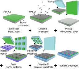
What They Say Perovskite-info.com reported a new R&D project to develop a new patterning technique for the production of perovskite nanocrystal displays which are ultra-thin and high-resolution. The technique uses a ‘stamp-like’ printing process. The team is said to have made RGB patterns at 2,550 ppi. The printed PeLEDs are claimed to have outstanding electroluminescence … Read more