At Display Week, I had the chance to moderate the CEO Forum and the panel included Nikhil Balram of Mojo Vision who told me that he had joined the firm partly to help it exploit the microLED technology that it has developed for its AR contact lenses.

 Balram is a very experienced display and semiconductor specialist that I had been aware of since he worked at Faroudja, twenty years ago. Since then, he has worked at Sage, NatSemi, Marvell, Ricoh and spent four years at Google in display R&D. He has been deeply involved in SID where he is a Fellow, since 2012, and was awarded the Otto Schade Prize. He was programme chair for Display Week 2019 and general chair for Display Week 2021.
So, I was pleased to catch up with his virtual talk at the SID/DSCC Business Conference to get a deeper dig into the technology. Although the primary purpose of developing its very, very high ppi microLED technology was to support the Mojo Vision contact lenses, the technology has a number of other possible uses and part of his role is to work on those. That should help to bring more resources to the technology and its development.
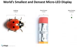
First to set, the scene, nothing like the displays needed for the Mojo Vision contact lenses existed, when development started. Balram highlighted how small the display is in this slide. The display is smaller than a dot on the ladybug/ladybird. The whole display is less than half a millimetre across.
 The Mojo Display is seriously small
After summarising the many benefits of LED, he highlighted that, eventually, LEDs will take over the entire display market, as LCD did with CRT. Balram segmented microLEDs as being either ‘dense displays’, with the pixels almost completely covering the area of the display (like microDisplays for AR/VR and Mojo’s own devices) and ‘sparse displays’ where the pixels are significantly separated (like TVs or monitors). His contention is that those that can make the dense displays will win the technology battle as they will have the technology to make very small pixels and can always spread them out further, gradually extending their reach as LCD did at one point to completely dominate every application.
Balram further split companies between those that can make very small (<2?m) pixels using the latest semiconductor techniques and larger emitters (>5?m) based on older processes. While the first group can address all applications, those with larger pixels can only address parts of the market. He said that investors see this and that ‘there is a big premium in valuation’ between the two groups.
So Mojo is in the first group and believes it is the leader and can make sub-micron pixels in RGB with efficient output. However, you have to be able to develop the backplane as well and the bonding, packaging and optics for creating good devices. Finally, you have to be able to get to high volume manufacturing using 300mm silicon processes to exploit the technology of the semiconductor industry. Balram said that it is strong in all these areas including using 300mm silicon wafers.
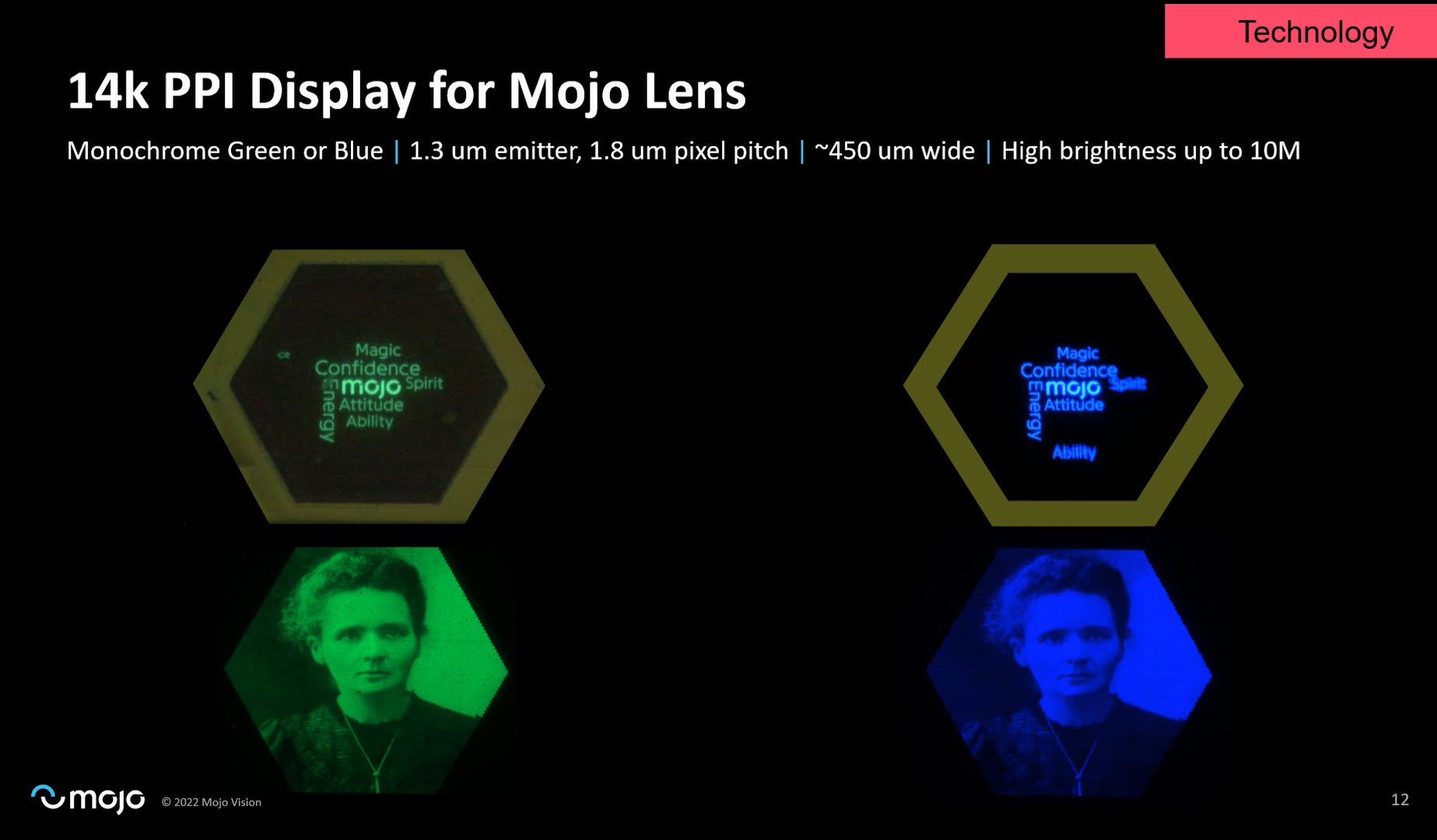
Looking at devices, the firm has made fully working green and blue 14K ppi displays with 1.3 ?m emitters and on a 1.8mm pixel pitch with high brightness (up to 10 million cd/m² for green) for AR/VR applications. The whole display is <0.5mm across. It has also made 20K ppi devices with 1 ?m emitters on a 1.3 ?m pitch. It has even made some 28K ppi devices, with a 0.6 ?m pixel on a 0.9 ?m pitch.
It is often said in the industry that you can’t make very bright, very small pixels with LEDs because of the increasing effect of non-radiative recombination at the edges of the pixel. A breakthrough for Mojo is that it has developed technology that solves the problem (although Balram didn’t detail it). That, lack of problems on the edge of the pixels, he said, is a big deal. Further, the I/V curve is the same at low currents, so the small pixels can be made at the same efficiency as larger ones.
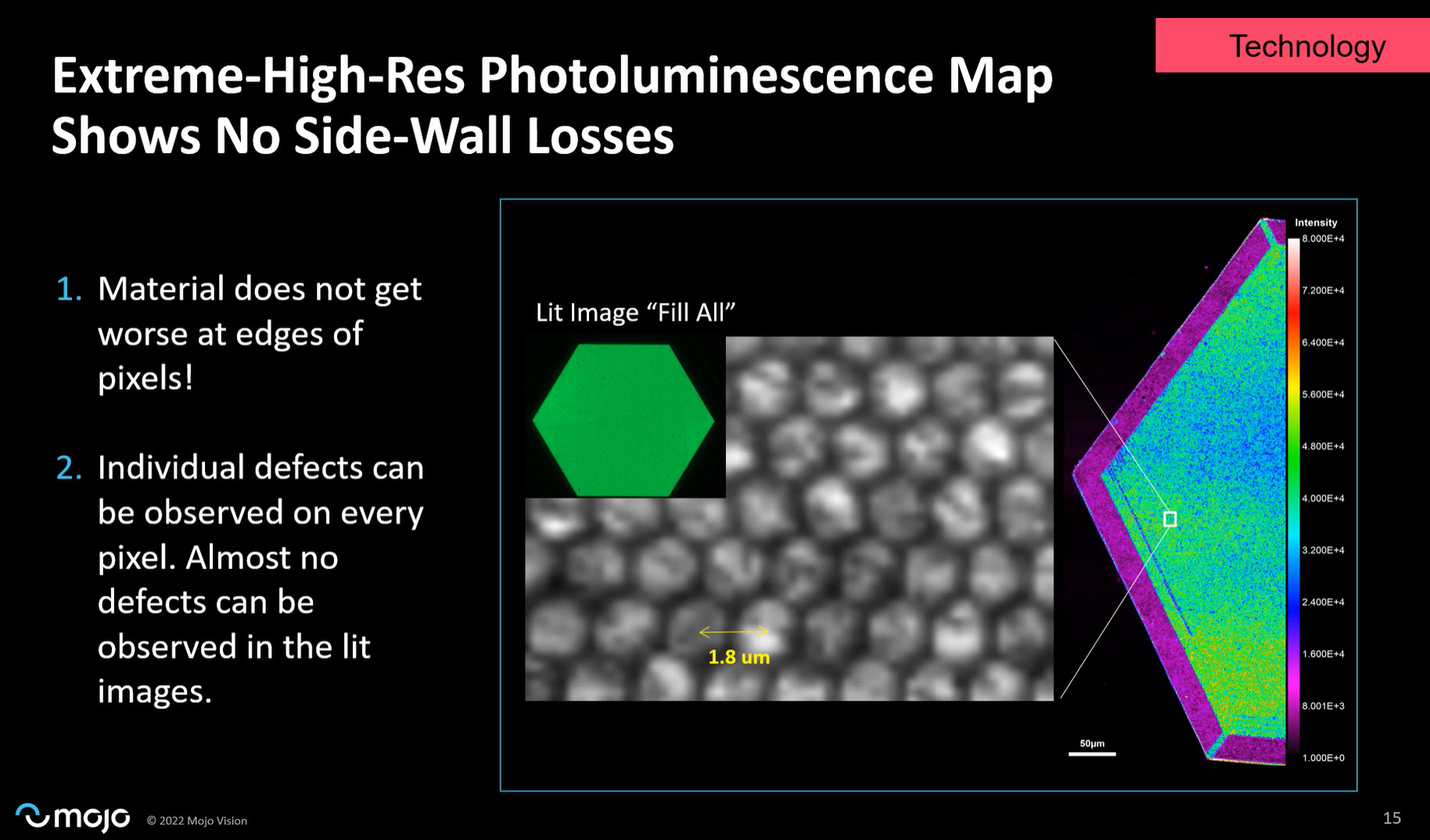 Although the pixels have visible defects, they are not visible and it can be seen that emission is from the whole of the pixel. Click for higher resolution.
The backplane from Mojo Vision is now in its third generation and it has a ‘random access’ addressing mode that only sends current to the pixels that are on. You have to support a wide range of brightness for AR to deal with the potentially high ambient to night time conditions and control has to be better than traditional PWM. Mojo has IP in this area. It’s good to be able to correct there, rather than having to ‘fix everything in the emitter’.
High volume manufacturing is possible because the backplanes and frontplanes with the emitters both use 300mm wafers, with the emitters using GaN on silicon. In the diagram, there is a stage marked ‘colour processing’ to create the pixels in R, G, B visible light, but Balram did not specify how this is done in his talk.
Analyst Comment
A lot of what Balram said in his talk make a lot of sense and do position the company as being in a very strong position. For example, his comment about segmenting the market is a good one. Back in the day when I was heavily involved in technology marketing, I spent a lot of time and mental effort on deciding the best segmentation. As Balram said in his talk, the right segmentation can really help you understand how to develop and exploit the market.
His points about the performance of the Mojo pixels at sub-micron size are also good. If the company can reliably make this size of pixel with high efficiency, it should certainly have success. (BR)