The Holst Centre in the Netherlands has developed a new process for spatial atomic layer deposition (sALD) that might be able to replace physical vapour deposition (PVD) at the same – and potentially even higher – throughputs. It may also be possible to perform the process at atmospheric pressure.
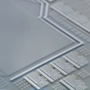
The Centre said that a key step in producing next-generation UltraHD displays is the creation of a highly uniform layer of an amorphous oxide semiconductor such as indium-gallium zinc oxide (IGZO). Today, this is typically done using a PVD technique known as sputter deposition. Sputtering requires expensive vacuum equipment and can also prove difficult to correctly control material composition and thickness over large areas. This results in variable transistor performance, particularly in thin film applications such as displays.
 The team said that it has used the technique to create semiconductor layers with charge carrier mobilities (a key measure of semiconductor performance) of 30 to 45 cm²/Vs. This compares to typical mobilities around 10 cm²/Vs for sputtering. The sALD layers is claimed to have exhibited low off current, switch-on voltages around 0 V and excellent bias stress stability.
“Spatial ALD offers all the performance advantages of traditional ALD – superior control of layer thickness and composition, large-scale uniformity and unparalleled conformability – but at 10-100 times the speed. So a typical 50-nm thick layer can be produced within the standard 1 minute window demanded by today’s industrial processes,” said Paul Poodt, Program Manager sALD at Holst Centre.
“The performance of sALD means semiconductor layers could become much thinner, enabling even higher throughputs and lower material consumption,” added Gerwin Gelinck, Program Director Flexible and Large Area Transistor Electronics at Holst Centre. “In fact, its performance characteristics are preserved even when scaling down the semiconductor thickness to less than 5 nm. This can lead to novel semiconductor structures, such as super-lattices, with even higher electron mobilities.”
The Holst Centre team and partners are now taking steps towards the upscaling and commercialization of these sALD processes and related equipment.
Analyst Comment
We’ve recently reported that Korean panel makers are looking at switching to ALD for OLED encapsulation (Kateeva Bullish on Encapsulation – Koreans to Adopt ALD?). On the other hand, Veeco recently said that it was reducing its investment in the concept. (Veeco Reduces ALD Investment)