
In the realm of advanced electronic device fabrication, particularly for organic light-emitting diodes (OLEDs), the techniques of thin-film deposition play a pivotal role. Two primary methods dominate the scene: solution processing and vacuum deposition. Both methods, distinct in their approach and application, cater to the nuanced demands of OLED manufacturing.
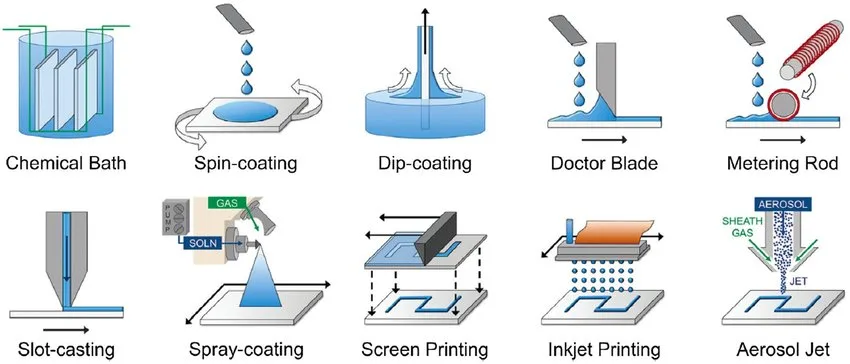
Solution Processing: An Economical and Versatile Approach
Solution processing, a technique involving the dissolution of materials in a solvent followed by application to a substrate, stands out for its cost-effectiveness and scalability. Techniques like spin coating, dip coating, and inkjet printing fall under this category. The simplicity of the setup and the method’s versatility with various materials and substrates make it an attractive choice, especially for large-area coatings. However, challenges in controlling film morphology, the complexities of solvent choice, and issues with purity and uniformity often mar its advantages.
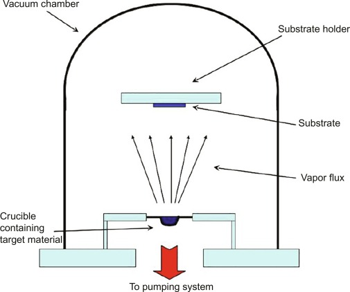
Vacuum Deposition: Precision and Purity in Thin-Film Fabrication
In contrast, vacuum deposition, which includes methods like thermal evaporation and sputtering in a vacuum environment, is celebrated for its precision. The control over film thickness, composition, and the higher purity and uniformity of the films are unmatched. Vacuum deposition is particularly beneficial for applications where ordered molecular packing and material efficiency are paramount. However, this precision comes at a cost, both literally and figuratively, as the method is more expensive due to its sophisticated equipment requirements and is less suitable for large-area applications.
IDT-CB: A New Frontier in OLED Materials
Transitioning from the theoretical to the practical, a recent study from the Universidad Nacional Autónoma de México showcases the synthesis and application of a novel indacenedithiophene derivative, IDT-CB, in OLED technology. IDT-CB was synthesized via a Suzuki coupling reaction, joining an indacenedithiophene (IDT) central core with two carbazole end units. Characterization with NMR and FTIR spectroscopy confirmed the anticipated chemical structure.
Measurements showed strong light absorption in the visible range and green-yellow photoluminescence from IDT-CB in solution. The compound was spin-coated into smooth thin films for incorporation into OLED devices. An OLED prototype with an IDT-CB emitter layer demonstrated bright yellow-green electroluminescence, with key metrics including a turn-on voltage of 5.76 V and peak luminance of 1000 cd/m2.
The results highlight IDT-CB as a versatile new material that can be deposited using simple and scalable solution processing methods. The successful demonstration of efficient electroluminescence from IDT-CB thin films opens doors for its future integration into practical OLED technologies and lighting applications. This novel compound demonstrates promising yellow-greenish light emission and exhibits a complex yet efficient electronic character. The research not only underscores the versatility of IDT-CB in various solvents but also highlights its stability and efficacy in thin-film form, a crucial aspect for OLED applications.
Reference
Álvarez-Venicio, V., Torres-Pérez, F., Guerra-Pulido, J. O., Cuellar-Pérez, S. N., Bernal, W., Martínez-Flores, C., Basiuk, V. A., Maldonado, J.-L., & del Pilar Carreón-Castro, M. (2023). Synthesis and characterization of a new semiconducting indacenodithiophene-carbazole derivative with interesting optical and electronic properties. Journal of Molecular Structure, 137121. https://doi.org/10.1016/j.molstruc.2023.137121