Some weeks ago, QD specialist and microLED developer Nanosys and released the news that it was collaborating with organic TFT developer Smartkem on the development of backplanes for different display technologies. We followed up to find out more.

We spoke with Jeff Yurek, a long time contact at the firm and someone that has helped us produce some interesting Display Daily articles on colour in displays and Sri Peruvemba, another long time contact and occasional guest contributor to Display Daily. They are both listed companies, these days, so caution in their statements was the watchword! (correction – Nanosys is not listed – at least, not yet although we think it will! Will Nanosys Go Public?)
First, a bit of background for those that are not avid Nanosys watchers. The company is the (very) dominant supplier of Quantum Dot (QD) materials and technology (via licensing) for most of the QD-exploiting products on the market. Until very recently, the QDs were only used in films by LCD suppliers to colour convert blue light from LEDs to white for use mainly in TVs, but in monitors and other applications too. Samsung Display recently started using the colour conversion technique with QDs in its QD OLEDs that are converting blue light from OLEDs to red and green for TVs and monitors. Samsung has impressed all those that have seen its QD OLED technology, which has better saturation in high brightness than WOLED panels from LG Display.
However, the firm also has two big display development areas beyond LCD and OLED. One was something of a surprise to us when it said that it had bought the microLED developer Gl? last May. Gl? has been developing microLED technology, originally for microdisplays applications such as AR and VR glasses and we have reported in the past that the firm was working with Jasper of Taiwan, which made CMOS backplanes for this kind of device. Initially, the firm seemed to be just developing for this kind of monolithic microdisplay, based on the concept of ‘nanowires’ that it had been developing, but the firm was also looking at individual microLEDs that could be distributed over an area to make a bigger display surface.
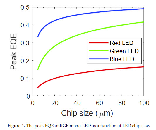 LED Efficiency falls with small LED chips. Source:CrystalsHowever, as we have reported several times, and as shown in the chart on the right from here, really small LEDs have a problem. As the sides of the LED get below 10 microns, the efficiency falls away very fast, especially for red. And you need to get the microLEDs that small if you want to drive down the cost of a display based on microLEDs to compete with LCD and OLED. So, the Nanosys purchase of Gl? is intended to allow the development of very small blue LEDs with relatively efficient colour conversion to red and green, overcoming the size issue. (although there are plenty more challenges, but that’s beyond the scope of this article).
ELQDs or NanoLEDs
The other area that Nanosys has been talking for a number of years about is the idea of electroluminescent QDs, which is to say QDs that are excited to produce light not by photons, as they are in colour conversion, but by electrons. That ought to be more efficient and simpler than converting the electrons to blue photons and then colour converting them. However, it’s not easy. Nanosys calls these NanoLEDs, but I’m going to call them ELQDs, for now.
Both the microLEDs and the ELQDs are emissive technologies that need active matrix backplanes if they are to be of high enough resolution and quality to be competitive with LCDs and OLEDs. That’s where Smartkem comes in, and, conveniently, for both technologies.
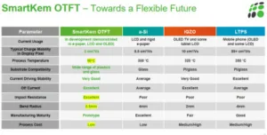
Smartkem has developed materials that can be used to make organic transistors. These transistors are better in performance than the amorphous transistors that are typically used in large LCDs, although less tricky and/or expensive to make than the main alternatives of oxide transistors and polysilicon. In the last couple of years Smartkem has moved some of its development efforts to making backplanes for active matrix backlights as the transistors are capable of conducting significant current, making them a good match for that application. The same property make them suitable, too, for driving other emissive technologies, such as microLEDs and ELQDs. As I said in my article last year (You’re Going to Hear About Smartkem Again),
“It seems to me that Smartkem has also shown that its materials could also be used to make direct microLEDs”.
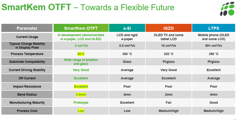
If you can make transistors that are robust enough to drive the level of brightness needed for backlights to LCD displays, where around 95% of the light is thrown away, you should have no trouble driving microLEDs or ELQDs!
The Manufacturing is Different
The second key point is that these organic materials can be made into inks and printed using low temperature processes and with a range of printing techniques including spin, slot-die and ink jet printing. The processes can be implemented in existing LCD fabs, but if starting from scratch could be used to build new fabs that could have significantly lower cost, especially when compared to IGZO or LTPS fabs. Essentially, it’s a clean set of printing systems that you need. There is even talk of roll-to-roll (R2R) manufacturing being possible – and that has long been a dream of display makers that want to make very cheap, very large flexible displays (although I have heard this so often over the last two decades without anybody ever getting close that I tend to discount it until I see it!)
Low temperature processes can also be important because it means that you can add the transistors to an existing display device after manufacturing, rather than the other way around, even if the display device is very heat sensitive. That gives you more flexibility and can help with issues of yield. If, for example, you have a tricky display making process, you can add the transistors afterwards. That would mean that if the display element was defective, you are not throwing away a finished backplane that may have cost a lot.
The lower temperature also means great flexibility in the choice of substrate film that you might want to use. There are films that can withstand high processing temperatures (and by chance, Panasonic sent details of one the other day), but there can be disadvantages to using these in other performance areas such as optical quality or cost.
Shifting Supply Chains
The idea of lower cost (capex) fabs is very interesting as the world moves away from global supply chains after the various shocks of recent years. There is a desire to move to more regional manufacturing, with displays possibly being made in the US and Europe as well as in Asia. That desire is not just within companies, but also within governments.
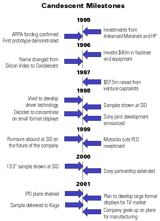
However, especially in the US after the experience of VCs with Candescent Technologies, VCs are not keen on huge display fabs. For those that don’t have my long memory (and big database!), Candescent was a Silicon Valley start-up that backed one of the competitor technologies to LCD and OLED, that of FED. The firm raised $600 million including $170 million from Sony and ‘at least’ $25 million from HP. It struggled to make the displays and by the time it got close to production, the fab it had built was making the wrong sized displays. After it gave up, in December 2001, the ip went, if I remember correctly, to Sony, which then spun it out before it all came to an end after some impressive demos in 2007 at Siggraph. US VCs have not looked kindly on big capital investments in display fabs ever since and II remember that this one of the largest ever VC funded start-ups in history at the time.
(I found the timeline on the right in my article from that time!)
Anyway, the thought that the US or other regions could get back into display manufacturing with a much lower level of capex than the $5 or $6 billion that it might need for a large IGZO plant is clearly an interesting one. Up to now, as NEC highlighted when it got out of volume LCD market share chasing nearly 20 years ago, the key to being in the display industry was to be prepared to bet huge amounts on the backplane technology. Having the right quality and technology of backplane has been, for a long time, the key to industry success. I remember Bruce Berkoff saying at a conference, when he was at LG Display, probably 20 years ago,
“I don’t care what kind of display you put on my backplanes”
Transistor size and Exclusivity
Getting back to the technology I asked my interviewees if there were any issues with the size of the transistor being too big for very small displays in any way, but Peruvemba confirmed that there had been no applications, so far, ‘where the transistor size is a limit’.
I also asked about any exclusivity from either direction and Nanosys said that it was not making any comments about this deal but pointed out that, historically, it had not made exclusive deals for its technologies or materials.
From the Smartkem side, it seems to me that this kind of deal was almost a ‘no-brainer’. Nanosys is a very well established part of the display supply and technology ecosystem with a strong reputation for its understanding and knowledge. To get the firm’s public endorsement for even the possibility that Smartkem could have something significant is a big deal indeed, at this stage of the company’s development. (and it also had endorsement from RiT Display in Taiwan, which is working with Smartkem on OLEDs (Smartkem On the Up with RiTdisplay JDA)
And, of course, Smartkem recently started trading its stock on the US OTCQB market (SmartKem, Inc. Begins Trading on the OTCQB in the US). It might be seen, by some, as a US company, then, although its staff and facilities are in the UK (apart from my interviewee!). (BR)
(This article was independently produced by Display Daily, but has been moved outside the paywall by Nanosys, so that it does not count towards your free allowance if you are not a paying subscriber. Thanks to them.)