This Display Daily article has several starting points. The first is the fact that technology based on plasmonics has not yet been used in any large scale commercial applications. A second starting point is that it is desirable to simultaneously improve the efficiency and stability of OLED device technology. This article will report on a third starting point, work undertaken by a team of researchers from Universal Display Corporation (Ewing, NJ) to use of plasmonic effects to improve OLED device performance.

A recent article on this subject by the researchers was entitled “Plasmonic enhancement of stability and brightness in organic light-emitting devices.” It was published in Nature ;585, ;379-382 (2020). A copy of the article is available for purchase and can be found here.
First a few words of background information.
Regarding plasmonics: Plasmonics is the study of the resonant interactions of electromagnetic waves and free electrons in solid state materials. Surface plasmons exist at the interface between a metal and the surrounding dielectric environment. These collective oscillations of electrons along the metal surface result in large electric fields and in an orders-of-magnitude improvement in decay rate of the oscillations over the visible spectral range making them well suited for use with OLEDs.
Regarding OLEDs: Part of the problem with OLEDs, even those incorporating organic phosphors that achieve an internal charge-to-light conversion of 100%, is that their refractive index mismatch reduces the fraction of light that makes it outside the device to around 25%. Furthermore, during OLED operation, a localized build-up of slow decaying triplet excitons and charges gradually reduces the brightness of the device in a process called ageing, which can result in “burn-in” effects in display applications.
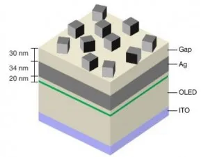
The means developed by the researchers to address these issues uses the decay rate enhancement of a plasmonic system to increase device stability, while maintaining efficiency by incorporating a nanoparticle based out coupling scheme to extract energy from the plasmon mode. This plasmonic OLED approach, which the researchers call a plasmon NanoPatch Antenna (NPA) approach, is depicted schematically in the figure below.
 Configuration of the plasmon nanopatch antenna device.
In the figure, the nanoparticles are represented as Ag cubes having a fill factor of 15% and a center to center spacing of about 200nm. Using finite difference time domain modelling, the researchers expect that by going from randomly arranged nanocubes to periodic or quasiperiodic cube arrays, the device out coupling efficiency could be further enhanced and tailored for directional emission.
In accelerated constant current density ageing tests, the plasmon NPA was found to achieve a nearly three-fold stability increase compared to a reference OLED incorporating organic phosphors that are similar in layer structure to commercial devices. This dramatic enhancement in device stability was achieved without loss in efficiency.
In summary, the researchers have demonstrated enhanced OLED stability by improving the decay rate via surface plasmon coupling, a strategy that the researchers report is usually considered detrimental to overall device performance. The new approach to increasing OLED stability avoids material specific designs and is applicable to all commercial OLEDs that are currently used for applications – including displays. -Arthur Berman
Universal Display Corporation, Nicholas J. Thompson, [email protected]