

At the DSCC/SID Business Conference this year (with access still available until September), Helander slightly re-positioned OTI as a company that is targeting the areas of an OLED that are not ‘the organic stack’. But his talk went well beyond his own firm’s materials and looked at the different strategies for under-display cameras, so after Oppo put out a release last week about its developments in this area, I thought it was worth looking at his talk again. (Oppo Unveils Next-Generation Under-Screen Camera Technology). It was a 45 minutes talk, so this article is very condensed.
The key driver for the move to under-display cameras is the desire to increase the display area on the front of a smartphone and eliminate the display notch, cut-out or hole. Further, if you can move the camera to under the display in devices such as notebooks, you can improve the experience of video conferencing by putting the camera into the eyeline of the user.
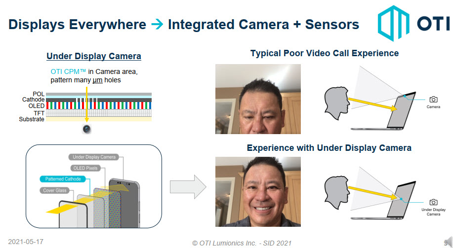
The key to developing the Under-Display Camera is to make the display sufficiently transparent to allow the effective transmission of light (both visible and infrared) through the display. For rapid adoption, you have to solve several problems. In the case of infrared (used for face recognition etc) the light has to go out through the display, bounce off the user and then get back through the display, compounding the challenge.
Helander looked at five specific challenges.
-
The Polariser
Removing the circular polariser is one solution, by simply cutting a hole in it but that changes (and typically degrades) the performance of the display in that area. Other alternatives include using a different polariser material for the camera area, but that is difficult to do in mass production and is likely to lead to an obvious transition area between the materials. You could try the kind of techniques used to replace the polariser (see OTI Lumionics Helping With Foldable OLEDs) but you have to remove the black matrix material in the region of the camera to allow light transmission and again this leads to visible differences in the display.
-
OLED Pixels
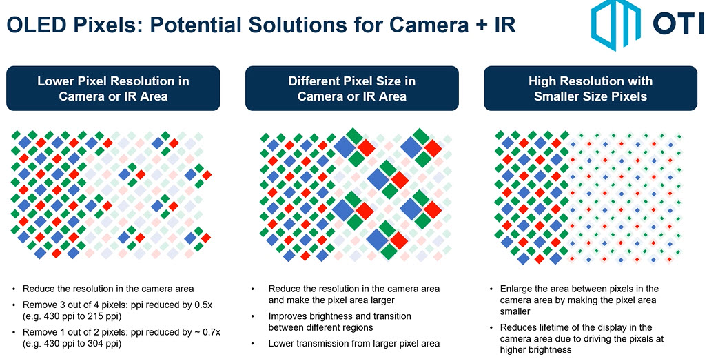
As the resolution of smartphone panels increases, the OLED pixels get smaller and there is less space for the light to travel through. Potential solutions include simply reducing the pixel resolution in the camera area. However, that reduces the resolution and brightness. You can restore some brightness by using bigger pixels in that area, but you still lose resolution. Alternatively, you can maintain the number of pixels, but make them smaller. That solves the resolution issue, but the display will lose brightness or lifetime if you drive the pixels harder to equalise brightness. (Interestingly, DSCC has pointed out that the trend for higher resolution has gone into reverse in smartphones in recent years, but that’s probably a topic for another article!).
-
TFT Backplane
If you have higher resolution, you still need a lot of TFTs and they can cause diffraction issues which reduce the performance of the camera as well as blocking some light. Solutions can included moving some of the TFTs to increase the density around the edge of the camera area, but that doesn’t work well in high resolution displays. A second approach is to use fewer TFTs in the camera area so that one transistor drives several pixels. Again this reduces resolution and adds visible transition areas. A third approach combines these two approaches, but with similar downsides in both areas.
-
Polyimide (PI) Film
Flexible OLEDs are made on PI substrates which is flexible but is slightly yellow. That’s not a problem for the display as the PI is behind the pixel, but it will affect the light going through the film to the camera. You can use a laser to ablate a hole in the PI film, but it is difficult to do in mass production and you can damage the TFT or barrier film in the process. You can thin the PI film in that area, but again it’s tricky in mass production. An alternative is to switch to colourless PI, but that material is not compatible with the LTPS processing typically used for flexible OLEDs, and is much more expensive which is a challenge in itself. (In a follow up interview, Ross Young of DSCC and Helander discussed the potential for using AI to sort out the yellow problem, but there are challenges in doing this in a mobile device at the moment).
-
Cathode Metal
The cathode metal layer of Yb/Mg/Ag typically covers the whole area of the display in flexible OLEDs. That’s a moderate issue for visible light cameras, but is a critical issue for IR sensors. Even very fine metal lines mean very low transmission of IR and reflection from the metal layer as well as diffraction problems. This is exacerbated by the need for the IR to go through the display twice.
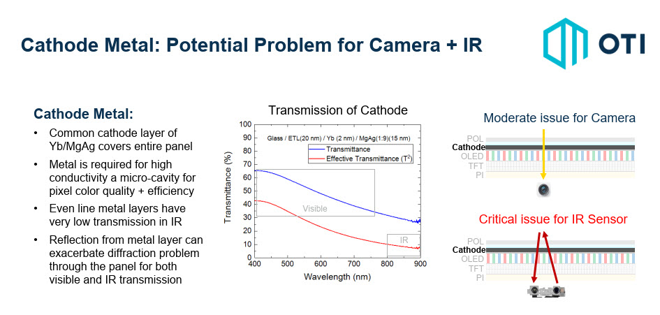 You can see from the graph in the centre that IR has a big challenge.
Solutions for the cathode include changing to a transparent cathode material such as an oxide. Unfortunately, the sputter process used to deposit those materials typically damages the OLED pixels and the device performance is lower than using metals. Further, the metal layer acts as an optical microcavity by reflection, so removing it reduces the OLED performance. Another possible solution is laser ablation, but again there are potential damage issues that can cause low yield. There is also significant capex expense for the process. This is where OTI’s CPM material, that we described last year, really comes in.
OTI said that ‘its customers’ customers cover 95% of devices, so is clearly working with Samsung among others, although no names have been released. It would be interesting to know if Oppo is using something like the OTI materials.
The firm also presented a paper (23.3) at Display Week on applications in larger displays and perhaps I’ll return to cover that topic. (BR)