
A team of researchers from Shanghai University recently demonstrated a technique to improve the integration and performance of tiny MicroLED devices for next-generation displays. Shrinking LEDs to the micro scale introduces manufacturing and reliability obstacles. A central challenge is integrating arrays of MicroLED pixels with the silicon control circuitry that operates the display. This is achieved using a process called flip-chip bonding that physically and electronically connects the MicroLED chips to bond pads on the silicon backplane. As pixel sizes shrink below 50 micrometers, this bonding interface can easily fail due to tiny defects and mechanical stresses.
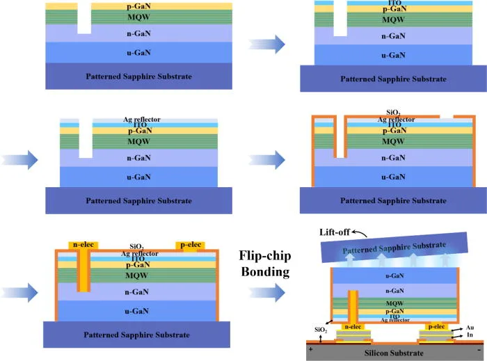
The Shanghai team aimed to enhance the flip-chip bonding process by using a layered gold-indium-gold (Au/In/Au) metal sandwich in place of conventional pure indium bumps. Flip-chip bonding then joins the MicroLED to the silicon at mild 200°C temperatures, avoiding damage from heating and cooling mismatches while forming highly conductive bonds.
According to the research, this multilayer approach reduced electrical resistance by 40% compared to pure indium, while also eliminating cracks and gaps at bonding surfaces. Testing sheared strength showed the Au/In/Au bonds to be over three times stronger mechanically. The group integrated these layered connections into a working 15×30 pixel MicroLED demonstration array with 20×35 micron sized sources. The panels exhibited impressive performance including low operating voltages and record high brightness reaching 1.78 million candelas per meter squared.
Reference
Xiaoxiao Ji, Kefeng Wang, Haojie Zhou, Fei Wang, Luqiao Yin, Jianhua Zhang; The improvement of bonding metal layers for high resolution micro-LED display application. Appl. Phys. Lett. 11 December 2023; 123 (24): 241102. https://doi.org/10.1063/5.0177351