
Ross Young, CEO of DSCC started the Business Conference with a message that the last two years saw record breaking revenues, shipments and profits, but warned that it would take four years before the industry returned to 2021 performance. The good news is that for the first time ever, there are two strong technologies and MicroLEDs are on the way.

Given the competition, both LCDs and OLEDs are upping their game, and after 20-years, OLEDs are hitting their stride having enabled new rollable and foldable formats, a doubling of performance and nearing a solution to the ”blue” problem.
Display Industry’s Record 2021 to be Followed by 2022 Hit by Geopolitical and Excess Capacity
Young’s keynote reiterated the OLED Association’s point that 2022 would be a negative growth year, diminished by too much large area capacity growth in China causing a drop in panel prices without an offsetting increase in demand because of unprecedented 2021 TV and IT panel buying. Young further laid the blame on inflation, slowdowns in China, the cost and transport increases caused by the supply chain crisis and the Ukraine-Russia conflict, which is lowering demand, causing a shortfall in wheat, other staples and minerals, where these two countries provide a preponderance of the supply. But while LCDs will fall in revenue and shipment volume, OLEDs are expected to thrive in smartphones, TVs and IT, leading to an assessment that the industry is now bifurcated, where OLEDs lead in the high-end, LCDs hold sway in the medium to low end and MiniLEDs are in the middle targeting the high end with less performance but higher costs than OLEDs. In the first Keynote, LG’s CTO Soo-Young Yoon pointed out how OLEDs outperform LCDs, but could very well have claimed victory for the technology while looking forward to the challenge of MicroLEDs.
LGD Fires Back at SDC with a 2,000 nit WOLED TV
The Samsung booth highlighted the color volume differences between QD-OLED and WOLED with a side-by-side comparison although Samsung was silent on their strategy of over driving to make the color pop regardless of the cinematographers’ input. (to be fair, Samsung Display was at SID – it’s Samsung Electronics that does the tone-mapping to make the TV look the way it does – editor).
LG Display fired back with a 77-inch 8K 2000 cd/m² OLED TV, twice as bright as conventional WOLED TVs. The new display is characterized by a fine convex lens array layer inside the OLED panel. The layer is not created by physically attaching an actual lens. A very thin lens material is deposited on the OLED panel through a deposition process and patterned to form a convex lens shape. The lens array layer adjusts the angle of light so that less is lost inside the OLED panel and amplifies it to increase light efficiency. It is a method of adjusting a light path so that light reflected from the inside of the panel advances toward the screen.
Previously, it had been rumoured that LG would use a micro lens. LG calls this technology a meta-lit lens array (MLA). When MLA technology is applied, OLED luminous efficiency jumps by more than 20%. The viewing angle is widened by a light scattering effect. When viewed from the side, the screen is bright and clear. Its luminance reaches up to 2000 cd/m² at a 3% APL. The 77-inch 8K OLED TV was the world’s first TV using both EX and MLA technology. EX refers to the OLED.EX panel technology that LG Display unveiled last year. LG Display plans to apply MLA technology to premium large OLED TV models in the future. Shin Hong-jae, a research fellow at LG Display, made a presentation about research results on the principles and effects of MLA technology at this year’s SID.
(Barry made the point to me that there is a lot of confusion that different panels are quoted as having different luminance, but without specifying the APL used for the measurement. He would like to see a single value used for the APL when quoting the luminance, but my feeling is that this would not succeed in being adopted as different technologies/products do better or worse at different APLs. In the end, luminance in a colour system is way more complicated than a single number. The IDMS has lots of ways to characterise luminance – and as I have written, I favour gamut rings You Can Extend the Idea of Gamut Rings . There are, of course, certifications that cover performance such as the VESA DisplayHDR labels for monitors. Those labels specify the luminance, but also specify test conditions. And, of course, there are two versions, effectively one for OLEDs and one for LCDs. – editor)
AR Displays – Meta Keynote Challenges the Industry– Your Displays Are Not Ready
Every few years, a keynote speaker comes along and challenges the industry to do something beyond its current level of competency. Joe O’Keeve, Meta’s VP of Display ad Optics did that last week. While the world listens to the leaders from Meta, Apple, Microsoft and Google rave about the brave new world of the Metaverse, the specs for an AR-worthy display remain unclear. Joe put an end to that with one chart.
He called on the display industry to provide displays at the upper left hand corner of the following figure and the figure shows why a see through AR, sometimes called XR, needs 6000 ppi, a 15 mm focal length, 500 nits to the eye and a duty cycle of 10% to avoid jitter when the user is in motion.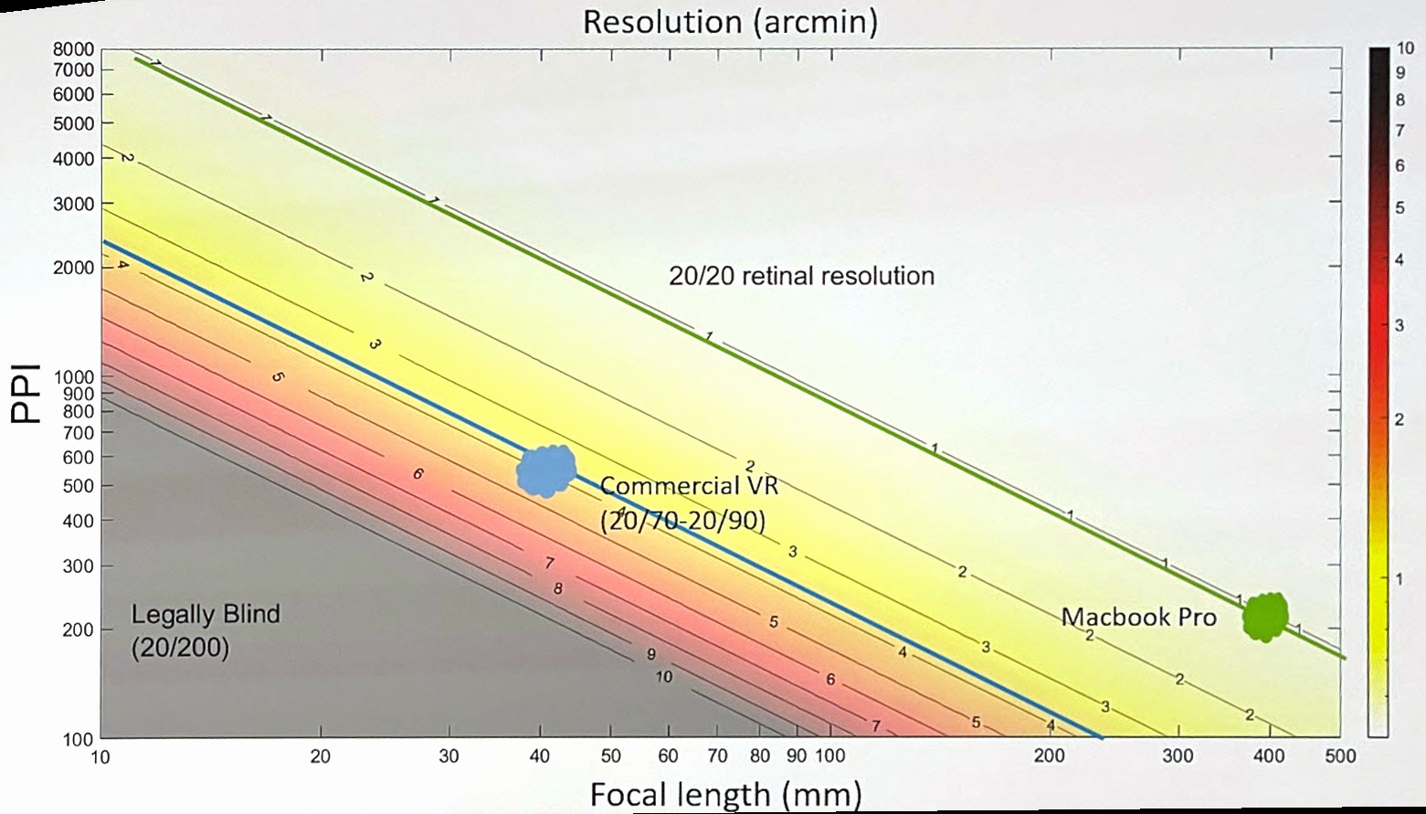 Figure 1: PPI vs. Focal Length – Source:Meta
Today, with a pancake lens, 3,000 ppi and 40 mm focal length is available. Orders of magnitude improvement are necessary and will likely involve a new lens and the commercialization of MicroLEDs or a giant leap in resolution and luminance for OLEDs to achieve the performance we want.
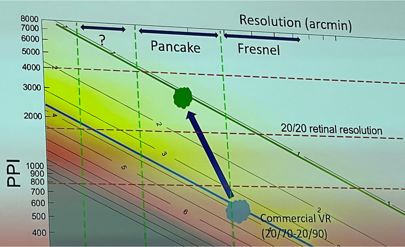 Figure 2: PPI vs. Focal Length — New Generation Lens Source: Meta
Although SID normally doesn’t distribute keynote addresses to its members, this is one that needs to be in the hands and minds of every member.
China’s OLED Program – A Failure to Perform
China dominates the LCD market with close to 70% of capacity and production. The previous leader, Korea, has thrown in the towel and except for two mid-level LG fabs, will be out of production by the end of 2022. But while Chinese panel makers have almost as much OLED small/medium capacity as the Koreans, they produce less than 30% of the volume and just recently suffered a major setback, when BOE tried to fool Apple, the largest buyer of small/medium OLED panels, into accepting an off spec model for the iPhone 14.
In large area OLEDs, Korea is the sole supplier and the on-again/off-again attempts by BOE and CSoT create questions about their viability to make OLED TV panels. Perhaps, TCL’s upcoming decision on whether to go forward with their IJP Gen 8.5 will provide positive answers. TCL demonstrated a 65” IJP OLED prototype TV with 8K resolution in their booth. The luminance was 600 nits (no APL for the test was provided), but two years ago SDC’s QD-OLEDs prototypes had even less luminance.
 Table 1: OLED Panel Production by Panel Maker – 2020-2021 Source: Omdia, OLED-A
MicroLEDs – A Cry for Leadership.
If we were only to use the OLED Exhibit Hall as a reference, PlayNitride, a young start-up with no commercial display products would be the leader. At the entrance to their booth, was a 132-inch tiled MicroLED that was completely seamless offering 2,000 nits and a 116% NTSC color gamut.
PlayNitride also showed a 9.38″ transparent display, with 65-70% transparency and an 11.6″ 24:9 2.5K resolution automotive-grade display.
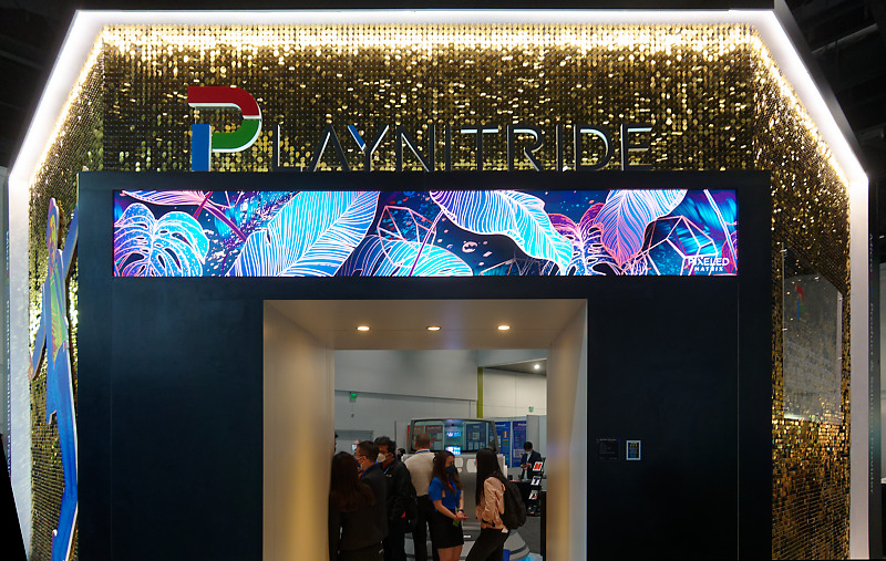 Figure 3: PlayNitride Entrance Image:Meko
The booth included a 1.58″ Passive-Matrix wearable display, a 7.56″ touch-enabled transparent QD-MicroLED display, a 1.39″ circular MicroLED and 7.56″ flexible panels and a 0.49-inch FHD (4536 PPI) full-color MicroLED micro display.
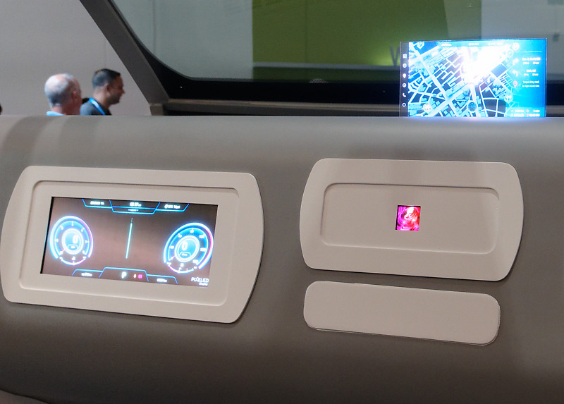 Figure 4: PlayNitride Automotive Displays Image:Meko
A number of the major panel makers had small MicroLED exhibits including AUO and BOE, but neither Samsung, Sony nor LG felt it was important enough to demonstrate their super large microLED TVs. MicroLEDs are being positioned as the future of the display industry, but there is no Samsung willing to lead and invest billions as they did in the 2000s to make OLEDs real. The most thorough roadmap is a very simplistic one from Yole, but lacks:
- Efficiency, lifetime and yield analysis for mass production
- Modeling of uLED costs by die and wafer size
- Mass transfer TACT and costs by resolution
- Evaluation of full color alternatives by type of application
Hopefully this will come as sales begin. DSCC forecasted the following:
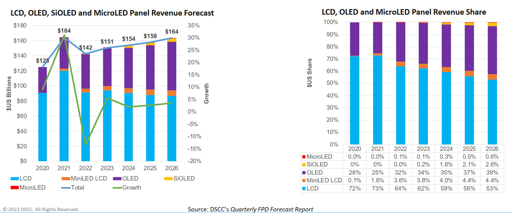 DSCC MicroLED forecast – Click for higher resolution
IGZO – LTPO on a Budget
IGZO is a backplane technology that falls between a-Si and LTPS in terms of performance (mobility) and cost. With a-Si at ~0.7 cm²/vsec and LTPS at 70 to 100 cm²/vsec, IGZO comes in at 10-12 cm²/vsec, good enough for 100-200 ppi, but not the high ppi’s used in mobile phones. Obviously, capex is dependent on the fab size but from a relative perspective, if a-Si is 1x, IGZO is 1.3x, LTPS is 2x and LTPO is ~2.5x. At DisplayWeek, Sharp announced it was making OLED displays for its latest Aquos smartphone using IGZO backplanes with 50 cm²/vsec, which delivers 456 ppi. (BY)
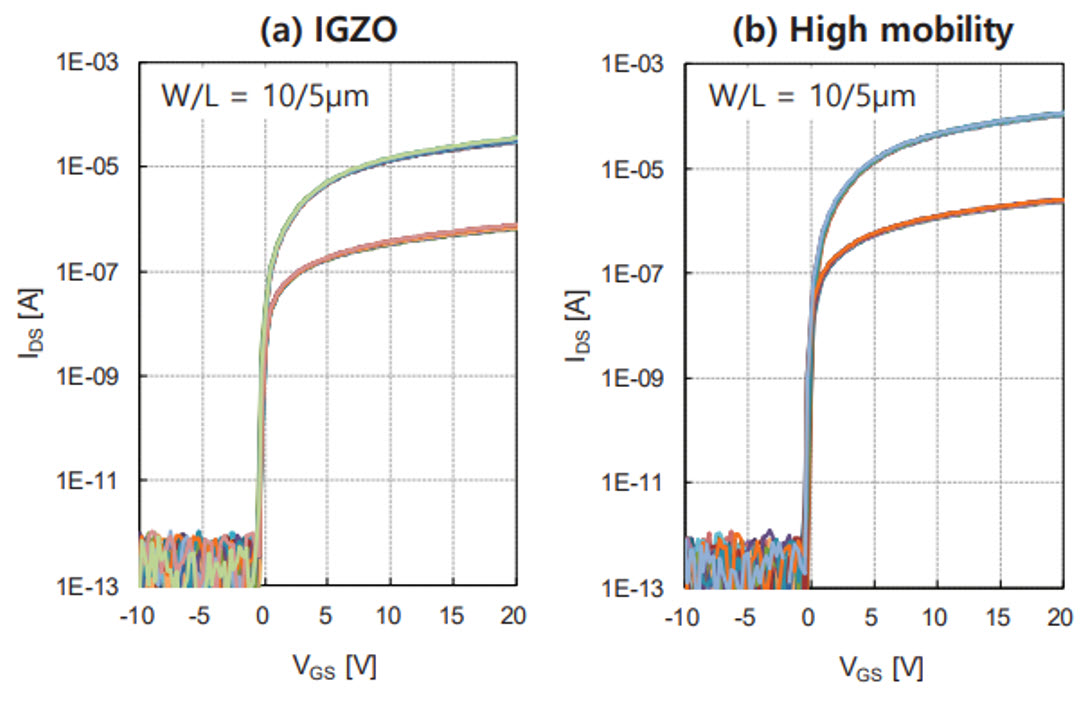 Figure 5: Transfer Curves of IGZO and High Mobility Oxides on Glass Substrates Source: SID Digest 2022 4-3 / J. S. Park
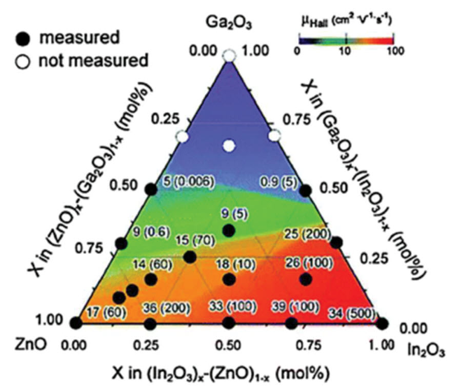 Figure 6: Electron Hall Mobility vs. Relative Cation Content (mobility increases under In-rich conditions) – Source: Kamiya T. et al. Origins of high mobility and low operation voltage of amorphous oxide TFTs: electronic structure, electron transport, defects and doping. J. Display Technology; 2009. vol. 5. p. 468-483. 7. Van de Walle C. G. et al. Vacancy defect
Barry Young is CEO of the OLED Association
This article along with Part 2 which will be published tomorrow, will count as only one article if you have a free access registration to Display Daily.