 Optovate has revealed further details of its innovative micro-LED technology, following its first technology announcement in March 2018.
Optovate has since 2008 been developing catadioptric micro-optic arrays to enhance the benefits of micro-LED, mini-LED and OLED displays and also a patterned laser lift-off (p-LLO) micro-LED transfer process. (see Optovate Comes out of Stealth Mode)
In a paper to be published at SID’s Display Week in LA in May, Optovate will present in more detail key benefits of catadioptric micro-optic systems for displays.

Optovate patterned laser lift off (p-LLO) process
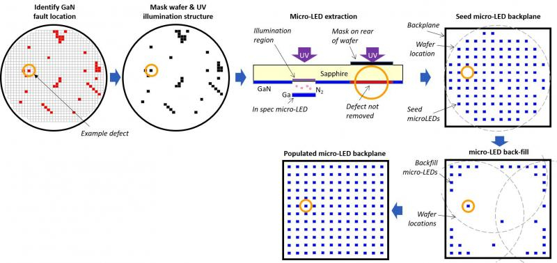
In parallel with the micro-optics developments, Optovate has made proof of concept demonstrations of its proprietary patterned laser lift-off (p-LLO) micro-LED transfer process and strategies for yield optimisation. Optovate’s p-LLO process used an excimer laser to illuminate sparsely separated die-sized regions of gallium nitride at the growth interface to a sapphire wafer. The UV exposure creates gallium metal and nitrogen gas which can controllably ablate the micro-LEDs onto a receiver tool or substrate.
Optovate was early to recognise the benefit of a selective array transfer process capable of dealing with variability across GaN wafers including growth defects, colour and forward voltage. The selective optical addressing capability of p-LLO enables pre-transfer characterisation data on wafers to be coded into the microLED extraction patterns and used for seeding and back filling microLED backplanes for yield optimisation. For microLED growth substrates such as silicon that aren’t transparent in the ultraviolet, Optovate also anticipated p-LLO process modifications in its IP, with the same performance enhancements.

Some elements of Optovate’s IP for micro-LED fault and array uniformity optimisation
Jonathan Harrold, co-founder of Optovate said:
“When we started work on what have now come to be known as microLEDs we were counter trend – everyone wanted bigger LEDs for lighting while we were predicting the future was sub 100 micrometre sized devices. That meant we had to develop our own manufacturing strategies for both microLEDs and micro-optics. The industry has now understood this and we are pleased to present results from those early IP insights”.
