Nine years ago, MicroLEDs were being touted as the next generation of displays, replacements for LCDs and OLEDs. That’s about 16 years after they were first discovered. Like most things in the display industry, this bright shining technology has been lauded and fawned over for years and it still looks like it is years away from being ready for mass consumer consumption. One of the frustrating things about the display industry is how much time is given to discussing technologies that move at a glacial pace but are treated in the present tense.
That’s not to say that MicroLED displays are not interesting or not making progress. They certainly are in some categories, particularly for near-eye displays, and small form factor devices like smartwatches. But, these developments come at a great cost to the manufacturers, and at great cost to the consumer. Both of these prices paid are don’t add up to any overnight success for MicroLEDs on the horizon, decades after they were created by Hongxing Jiang and Jingyu Lin.
Not All Microleds Are Created Equal
MicroLED technology can be categorized into two types of applications: high ppi (pixel per inch) and low ppi. High ppi applications include AR (augmented reality), VR (virtual reality), MR (mixed reality), head-mounted displays (HMD), and projectors. These applications require specific characteristics from displays, such as high contrast (100,000:1), high brightness (>5000 cd/m²), high ppi (>2000-3500, depending on who you talk to), lightweight, compact size, long operating time, high power efficiency, and fast response times.
For such high ppi applications, MicroLED displays are considered superior to both LCD and OLED. While LCDs suffer from significant brightness loss and are not suitable for HMDs and HUDs due to complex imaging optics, OLEDs are increasingly used in wearable AR systems but may not meet the brightness requirements for high-end glass-based AR/MR and HUD devices in outdoor environments. MicroLED, on the other hand, offers advantages of direct emission technology like OLED but with much higher brightness and ambient contrast ratio (ACR).
However, MicroLED technology, with its potential to revolutionize display applications, faces some challenges in its development and manufacturing. One such challenge is achieving high external quantum efficiency (EQE), which refers to the efficiency of converting electrons into photons in the diodes. This is crucial as higher EQE results in greater light output for the same amount of electrical power input. However, attaining high EQE in MicroLEDs is not straightforward, as it involves dealing with material defects, non-radiative recombination of charge carriers, and light extraction issues.
Interestingly, high ppi applications may encounter relatively fewer difficulties in achieving high EQE. The reason behind this could be that in high ppi displays, individual pixels are much smaller, reducing the impact of material defects and non-radiative recombination per pixel. High ppi displays often operate at higher current densities to achieve greater brightness levels. At these higher current densities, certain material defects, like sidewall defects, may become saturated, reducing their impact on the overall efficiency of the device.
Another challenge in MicroLED development is dealing with mass transfer defects. This issue arises during the process of transferring individual MicroLEDs onto the display substrate. Ensuring precise placement of each tiny MicroLED can be time-consuming and difficult, leading to potential defects or reduced display yield due to misalignment or damage during transfer.
However, high ppi applications may also see a potential solution to this challenge. In these applications, the individual MicroLEDs are significantly smaller, and the overall panel size is smaller as well. Monolithic integration offers a strategy to overcome some mass transfer defects in small display panels. This approach involves growing or fabricating the entire MicroLED array on the substrate as a single unit, rather than transferring individual MicroLEDs one by one. Monolithic integration simplifies the process and enhances the precision of placement.
Additionally, high ppi displays have the advantage of using higher current densities to achieve the desired brightness. Surprisingly, this can lead to another benefit for MicroLEDs: they outperform broad-area LEDs in terms of brightness at higher current densities due to lower efficiency droop. Efficiency droop is a phenomenon where external efficiency decreases at higher current densities, limiting the brightness attainable in broad-area LEDs. MicroLEDs, on the other hand, show lower efficiency droop, enabling them to maintain higher levels of brightness and overall efficiency at these higher current densities.
MicroLED technology also opens up possibilities for flexible and stretchable displays. By bonding tiny MicroLEDs to flexible or stretchable substrates, special displays like curved displays, foldable smartphones, and wearable electronics can be created. Transparent flat panel displays are also possible when MicroLED arrays adhere to transparent substrates with a low fill factor. This can enable applications like vehicle navigation and heads-up display (HUD) systems, where transparency is crucial.
| Manufacturing Method | Estimating First Implementation | Description |
| Mass Transfer | Early 2010s | This method involves the transfer of thousands to millions of MicroLEDs from a temporary substrate to a target substrate. |
| Laser Lift-Off | Late 1990s – Early 2000s | Using a laser to separate the MicroLEDs from the growth substrate so they can be transferred to a different substrate. |
| Fluidic Assembly | Mid 2010s | Relies on a liquid medium to pick up and place the MicroLEDs from a donor substrate to the target substrate. |
| Wafer Bonding | Late 2000s – Early 2010s | The entire MicroLED wafer is bonded onto another substrate and then etched away to leave the individual MicroLEDs. |
| Roll-to-Roll Transfer | 2020s | Involves transferring MicroLEDs from a roll of material to another roll. This method has the potential to be faster and more cost-effective than traditional methods, such as mass transfer or laser lift-off. |
To achieve full-color displays, the precise assembly of RGB monochromatic MicroLEDs requires a process of transferring thousands, eventually millions, of MicroLEDs onto a panel while ensuring accurate alignment, bonding strength, a formidable technical challenge. Currently, the existing transfer equipment and processes would take several months to produce a single 4K TV, making the realization of large-scale, high-resolution MicroLED displays not a thing. To address these challenges, researchers and industry experts are actively exploring mass transfer technologies that can meet the demands of the rapidly evolving display market.
When it comes to mass transfer, there are two options: direct monolithic integration and indirect pick-and-place methods. The direct monolithic approach involves directly hybridizing the MicroLED array onto the driving circuit through die-to-wafer or wafer-to-wafer bonding. This method is particularly suitable for high ppi applications but for low ppi applications, such as televisions and IT products, with large panels and a high number of MicroLEDs, the pick-and-place technology has been considered indispensable.
The main difficulty lies in taking each MicroLED from a source wafer, which is presently quite small, to a large panel while maintaining a high yield. This task requires greater percision than the industry has ever been used to because it requires that each MicroLED sits perfectly in its placed location, perfectly aligned with all the other MicroLEDs, forming a coherent display. Achieving such high alignment accuracy, bonding strength, and reliability on a large scale is nowhere near being achievable right now, and it may be that the pick and place method will never be capable of meeting the demands of consumer electronics and commercial displays using MicroLEDs.
There are numerous researchers and companies looking at alternative approaches:
Electrostatic Transfer Head
LuxVue, a company acquired by Apple in 2014, demonstrated the use of electrostatic forces to transfer MicroLED chips. The transfer head consists of a substrate with mesa structures and electrodes above the mesas, covered by a dielectric layer. By applying voltage, the transfer head can pick up MicroLEDs from the substrate and release them onto the receiving substrate. Is Apple anywhere near delivering MicroLED displays? No more than any other company, most without the benefits of Apple’s billions of dollars in cash.
Elastomer Stamp Transfer Printing
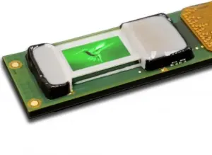
X-celeprint employs elastomer stamp transfer printing, where a compliant elastomer with a rigid glass backing is used as the stamp. MicroLEDs are formed on a sacrificial portion of the substrate and are then released and attached to the elastomer stamp. The MicroLEDs are subsequently transferred to the target surface by the stamp, relying on van der Waals interactions for adhesion. If you want to transfer 10,000 die at a time, you must have an elastomer stamp with 10,000 die-sized plateaus on it, with each plateau located within about 1µm of its target location. X-celeprint makes its masters using silicon wafers and photolithographic technology, a process that can easily achieve this level of accuracy. The stamp master is then used in a low-pressure injection molding system to produce the stamps used in production.
Beam Addressed Laser Lift-Off Release
Companies like Gl¯o, Uniqarta, QMAT, and Tesoro Scientific have taken a comprehensive approach to mass transfer, involving new materials, processes, and test equipment. MicroLEDs grown on a substrate are transferred to a laser-transparent carrier coated with a sacrificial layer. The laser then ablates a part of the sacrificial layer, enabling the MicroLEDs to be released onto the receiving substrate.
Fluidic Transfer
Fluidic transfer technology, developed by eLux (acquired by Sharp), utilizes a carrier liquid to transfer microLED chips onto a thin-film transistor (TFT) backplane. The microLEDs are captured in wells on the TFT substrate and then annealed to establish electrical connections.
Wafer Bonding
There are several techniques for wafer bonding of microLEDs, and the choice of method depends on factors like the material composition, desired alignment precision, and the scale of production. Some common wafer bonding techniques include:
Direct bonding: This method involves bringing two wafers into direct contact under controlled pressure and temperature conditions. If the surfaces are suitably prepared, they can form a strong bond without the need for additional adhesives.
Indirect bonding: In this approach, an intermediate layer, such as an adhesive or a metallic bonding layer, is applied between the two wafers to facilitate bonding. After alignment and joining, the intermediate layer is cured or activated to achieve a stable bond.
Eutectic bonding: This technique is used when the wafers have different thermal expansion coefficients. By creating a eutectic alloy between the wafers, a strong bond can be achieved even when exposed to temperature variations.
Roll-to-Roll Transfer
The MicroLED arrays are first grown on a growth substrate, which can be a standard semiconductor wafer or another suitable substrate. Epitaxial growth involves depositing layers of semiconductor materials to form the LED structures. A release layer is typically added to the top of the MicroLED array on the growth substrate. This layer serves as a sacrificial layer that allows for the subsequent transfer of MicroLEDs to the receiver substrate.
The growth substrate with the MicroLED arrays and the release layer is temporarily adhered to a carrier substrate, often a flexible or rigid support material that can be wound onto rolls. The carrier substrate with the growth substrate and MicroLED arrays is then fed into the roll-to-roll equipment. The release layer is activated by heat, laser, or other methods, causing the MicroLEDs to delaminate from the growth substrate. As the carrier substrate with the delaminated MicroLEDs moves through the roll-to-roll equipment, the MicroLEDs are transferred and bonded to the receiver substrate, which can be another flexible or rigid substrate.
Once the MicroLEDs are successfully transferred to the receiver substrate, the carrier substrate is removed, and the process can be repeated for continuous production.
It is very likely that roll-to-roll transfer methods will end being the ultimate method of commercializing MicroLED manufacturing. But, we have been here before, talking about a definitive path to mass production. What we do know is that research continues into all methods. We covered a recent paper on fluidic transfer that touted some advances, even though it is still a far cry from being applicable for TV or IT product displays.
The Path to MicroLED Commercialization Remains Rocky
It is one of the ironies of MicroLED technology, and a reason why it’s not ready for prime time, that the very things you can, in theory, overlook in near eye displays become blockers in larger displays. The biggest problem is that the display industry does not have any reliable or meaningful way of mass producing large MicroLED displays, no matter how low the ppi. Most of the well-known manufacturing methods, listed above, are unsuited to producing error free MicroLED displays for IT products and TVs.