The advent of semiconductor MicroLEDs has paved the way for advancements in spatially modulated imaging, optical wireless communications, wearable/implantable optoelectronic displays, and biomedical sensor systems. However, their integration onto non-native substrates has posed a challenge for mass production, hindering their deployment in devices such as televisions, smartphones, tablets, and flexible substrates like smart wristbands. Fortunately, Scientists from the University of Strathclyde in the UK have made significant progress in addressing the challenge of transferring micrometer-scale semiconductor devices onto various receiving platforms. Led by research team leader Eleni Margariti, the team has developed a roller-based printing process that enables the scalable and highly accurate integration of these devices.
In a recent publication in the journal Optical Materials Express, the researchers demonstrate that their innovative roller technology can achieve an impressive accuracy of less than 1 micron in matching the designed layout of the devices. Moreover, the setup is cost-effective and straightforward, making it accessible even in locations with limited resources.
Margariti highlights the broad applicability of this printing process beyond MicroLEDs, emphasizing its potential for other types of devices such as silicon-based electronics, transistors, sensors, antennas for flexible and wearable electronics, smart packaging, and radio-frequency identification tags. The method may also find utility in photovoltaics, drug delivery systems, biosensors, tissue engineering, and other biomedical applications.
The motivation behind this research stems from the limitations of current manufacturing techniques, where semiconductor devices are typically grown on wafers using deposition methods. Compatibility issues between the delicate thin film structures and suitable substrates restrict the versatility and performance of these devices. To address this, the team sought to improve the transfer process to enable the integration of a large number of devices with enhanced accuracy and efficiency.
The newly developed approach involves a loosely attached array of tiny devices on their growth substrate. A cylinder coated with a slightly adhesive silicone polymer film is then rolled over the suspended device array. The adhesive forces between the silicone and the semiconductor detach the devices from their growth substrate and align them on the cylinder drum. As the printing process is continuous, it allows for the simultaneous printing of numerous devices, making it highly efficient for large-scale production.
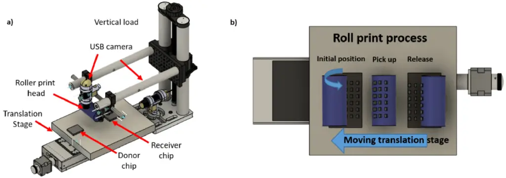
Margariti explains that meticulous selection of silicone and receiving substrate surface properties, along with the precise control of rolling speed and mechanics, enables successful transfer and placement of the devices on the receiver substrate while preserving their original spatial arrangement. To evaluate the printing quality, the team developed a custom analysis method that rapidly scans the printed sample for defects, providing valuable information on printing yield and positioning accuracy.
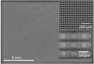
To validate their approach, the researchers focused on gallium nitride on silicon (GaN/Si) semiconductor structures, a dominant technology for MicroLED displays. Utilizing silicon substrates facilitated the preparation of suspended structures that could be easily picked up by the roller. Impressively, they achieved a transfer rate of over 99% for an array of more than 76,000 individual elements, with spatial precision below a micron and negligible rotational errors.
The research team is now dedicated to further enhancing the accuracy of the printing process while expanding the number of devices that can be transferred in each cycle. They also plan to investigate the method’s capability to integrate different types of devices onto the same receiving platform and explore its potential for precise printing to specific locations on the substrate.
With this groundbreaking roller-based transfer printing method, the researchers have unlocked new possibilities for large-scale production of MicroLED displays and opened avenues for advanced electronic systems and diverse applications in electronics, packaging, energy, and biomedical fields. As they continue to refine and advance this technology, the future of MicroLEDs appears even brighter.
Reference
Eleni Margariti, Gemma Quinn, Dimitars Jevtics, Benoit Guilhabert, Martin D. Dawson, and Michael J. Strain, “Continuous roller transfer-printing and automated metrology of >75,000 micro-LED pixels in a single shot,” Opt. Mater. Express 13, 2236-2250 (2023) https://doi.org/10.1364/OME.483657