François Templier, Research Director and Strategic Marketing Manager for Photonic Devices in the Optics and Photonics department of CEA-Leti, discussed his organization’s work at a seminar at Colombia University in New York on October 5th titled “GaN MicroLEDs for High-Brightness Microdisplays and Large Area Displays.” Besides his duties at Leti, Dr. Templier is also Director of the French chapter of the SID. Most of his talk was about microdisplays, not large area displays, and that will be the focus of this Display Daily.
![]()
 Dr. François Templier Discussing Hybrid GaN Microdisplays at Columbia (Credit: M. Brennesholtz)
Leti is a technology research institute founded in 1967 and is currently one of three divisions of CEA Tech. CEA Tech is a French research institute which, much like IMEC in Belgium, Fraunhofer in Germany or ITRI in Taiwan, specializes in partnering with industrial companies for state-of-the-art research projects. Leti focuses on micro- and nanotechnologies and their integration into systems. Of the 1900 scientists at Leti, about 200 are involved in opto-electronic systems, such as GaN-based microLED microdisplays.
Templier said one of the advantages of microLED over OLED microdisplays is the much higher brightness the inorganic microLEDs can achieve, compared to OLEDs. He said this added brightness is especially important for see-through Virtual Reality (VR) head mounted displays (HMDs). There are other applications where microLEDs could be better than OLEDs, including automotive head-up displays (HUDs) and virtual reality (VR) HMDs, he continued. Because of their high energy efficiency, microdisplays based on microLEDs may also be a good solution for small battery powered direct view displays that need to be visible in direct sunlight, e.g. smart watch displays.
Dr. Templier and Leti are focusing on hybrid microdisplays where an array of microLEDs from a GaN wafer are transferred en masse from the GaN substrate to a silicon substrate. We have reported on this before (subscription required) and reported on the Gen 2 monochrome blue WVGA (873 x 500) microdisplay from Leti with a 10µm pitch. This was produced by the process shown in a paper presented at SID 2017 and had an active matrix CMOS backplane. In his talk at Columbia, he went into considerable detail about exactly how the transfer process works.
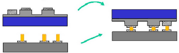 Flip-Chip assembly process with microtubes (Credit: Leti)
Dr. Templier said that with a classical hybridization technique, i.e. flip-chip with an indium bump, there is a pitch limitation of about 15 ?m. This isn’t really a fine enough pitch for most commercial microdisplay applications and another solution is needed. The Leti solution to this problem is called the microtube approach. He said that microdisplays with the microtube technology are currently showing a 10 ?m pitch, with Leti working towards 5 ?m.
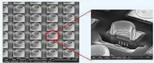
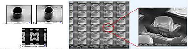 Left: (a) 4µm (b)2µm and (c) star microtubes; Center: an array of mictotubes; Right: cutaway image of a single microtube. (Credit: Leti)
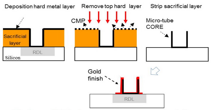 The microtube fabrication process (Credit: Leti)
Templier said the microtubes were formed with a photolithographic process, as shown in the image. The microtubes are made on the silicon substrate out of a hard material such as tungsten. On the flip-chip GaN wafer with the microLEDs, the pads are made out of relatively soft materials such as indium or aluminum. When the two substrates are pressed together at room temperature, the microtubes embed themselves into the pads. This forms both the mechanical and electrical connection between the CMOS silicon array and the microLEDs. The typical force needed to embed the microtubes into the pads is a few milli-Newton per connection.
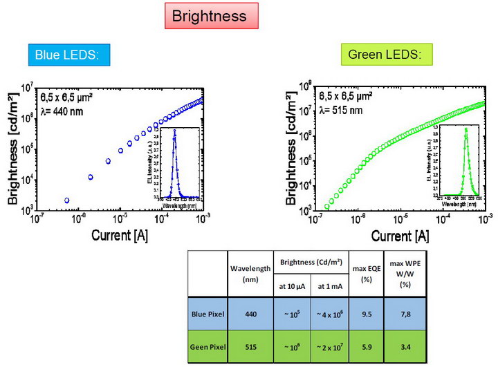 Characterization of Blue and Green microLEDs from the Gen 1 microtube display (10µm pitch, 300 x 252 array) (Credit: Leti)
The figure shows the brightnesses achieved at Leti for their Gen 1 blue and green GaN microdisplays using the 10 µm pitch microtube hybrid process and a 1-level connection silicon circuit backplane. Dr. Templier says that with their Gen 2 demonstration units, which also had a 10 µm pitch but used a 873 x 500 (WVGA) CMOS active matrix backplane, the blue units (440nm) produced 300 cd/m² while the green units (515nm) produced 10,000 cd/m².
![]() Pixel Pitches achieved by OLED production microdisplays compared to those achieved by microLED prototype displays (Credit: Leti)
Pixel Pitches achieved by OLED production microdisplays compared to those achieved by microLED prototype displays (Credit: Leti)
Dr. Templier said one of the key challenges for microLED microdisplays, regardless of whether they come from Leti or other research groups, is pixel pitch. Prototype microLED displays typically have a pixel pitch on the order of 10µm or so. In comparison, commercially available OLED microdisplay products from a variety of vendors achieve pixel pitchs of under 5µm today.
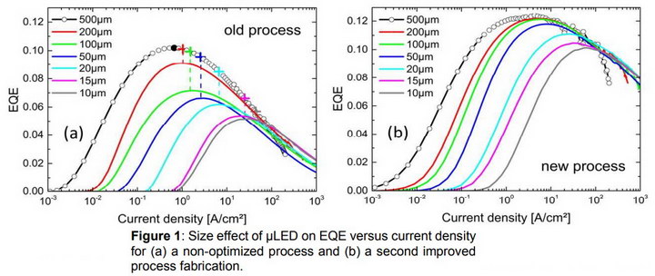 The External Quantum Efficiency (EQE) problem for small microLEDs has been reduced but not eliminated by Leti (Credit: SID 2018 Paper 59-4)
This microLED pitch problem is not just an assembly problem. As microLEDs become smaller, they become less efficient. Leti is working on this problem, and documented this improvement in an invited paper from Dr. Templier and his colleagues at SID 2018. With the old process, the EQE of 10µm microLEDs was about 5.5% while with the new process, the EQE is closer to 10%. This is still lower than the 12% achieved with the new process for large (500µm) LEDs, although it is about the same as the 10% EQE achieved with the old process with large LEDs. The problem is not just a manufacturing problem, it is a fundamental edge-effect. Since smaller microLEDs have more edge relative to the central area of the microLED, this pixel size vs. efficiency problem is never likely to go away completely.
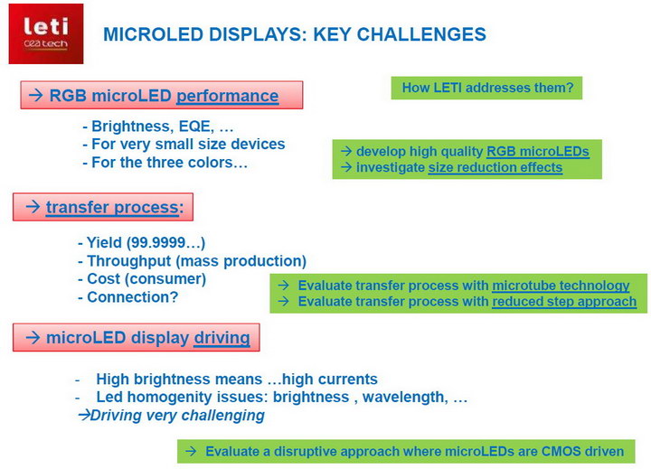 Key challenges for microLED displays and how Leti is addressing them (Credit: Leti)
Another challenge for Leti is the issue of a full-color microdisplay. Very few customers want either monochrome blue or green microdisplays for their AR or VR HMDs or their automotive HUDs. One possible approach to this is color conversion using phosphors or quantum dots patterned onto the individual pixels. Another solution, not discussed by Dr. Templier, is to follow one similar to the color-by-white process used by many OLED displays. MicroLEDs could use an unpatterned white color conversion material on the blue GaN backplane and then a color filter array.
A third option, discussed briefly by Dr. Templier, is to use mass transfer techniques to transfer separate red, green and blue microLEDs to a substrate. The Leti hybrid mass transfer method discussed in this article is not really capable of doing this, although the microtube approach to bonding the microLEDs to the new substrate is said to be suitable for this.
Another possible full-color approach would be to use three monochrome microLED microdisplays, GaN for blue and green and InGaAlP/InGaP/GaAs for red, and combine the three images for a full-color image. While this might be a solution for an automotive HUD, it probably would not be usable in a HMD.
Unfortunately for Leti, if a company wants to design an AR or VR HMD or an automotive HUD now for production in the near future, microLEDs are not a serious option compared to OLEDs or other display technologies. While research at Leti and other places may change this in the future, they are not commercially viable today for end-user products.
Templier said he has two invited talks scheduled for the near future at technical conferences. The first will be at the 2nd China International Micro-LED Summit to be held on Nov. 12th in Shenzhen and titled “Challenges for High-performance GaN MicroLED displays.” The second talk will be at Photonics West 2019 in San Francisco 2-7 February and will be titled “Advanced solutions for High-performance GaN MicroLED displays.” In these talks, he will discuss both further progress on microLED microdisplays and, hopefully, Leti’s work on large-area displays where the pitch of the microLEDs is not the same on the display as it is on the GaN wafer. –Matthew Brennesholtz