
CEA-LETI presented two papers at DisplayWeek and showed a demo in their booth on the show floor. Their papers described a new monolithic bonding technique and the booth showed the results.
In one paper, the LETI authors pointed that flip-chip bonding and direct GaN integration onto CMOS circuits is being pursued by several companies, but these seem to have a pixel pitch limitation of around 10 microns. For VR applications, where high density and lots of pixels are required, many believe pixel pitches in the 2-5 micron range or even smaller will be needed. To address the shortcomings of current approaches, LETI has developed a new monolithic bonding technique (Figure 1 below).
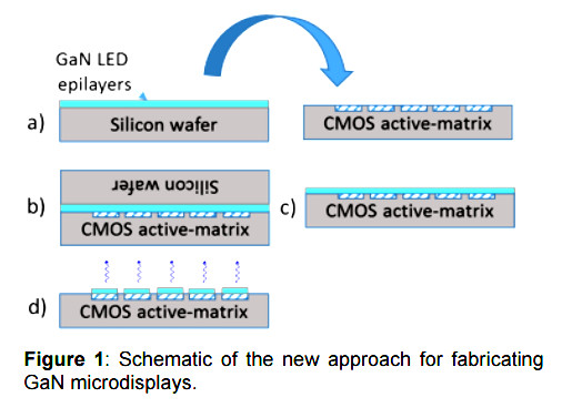
In the new approach, a GaN epi layer stack is grown on a silicon wafer and the stack flipped over and bonded to a wafer with a CMOS active matrix. The GaN stack consists of a p-type GaN layer followed by a multi-quantum well structure, n-type GaN layer and a buffer layer. The epi substrate is then removed via grinding and a plasma etch, allowing the LED array to be patterned and fabricated directly on the CMOS wafer. This avoids the alignment issues associated with previous techniques where the CMOS active matrix and GaN features are defined prior to bonding – which is the limiting factor in the 10 micron pixel pitch.
This new method allows the GaN devices to be fabricated on much larger silicon wafers and to use the latest semiconductor manufacturing techniques. One of the key innovations was the development of metal layers between the GaN epi layer and the CMOS matrix for good ohmic contact and good adhesion to the CMOS substrate.
To test the process, the epi stack was bonded to a metalized silicon wafer, not one with a CMOS active matrix. The multi-quantum well stack was designed for blue emission, but green and red can be designed too, which is how they will get to full color. Emission is created when current is applied between the top electrode of the defined microLEDs and the common anode.
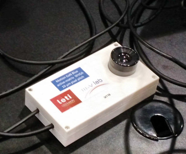
In their booth at SID, LETI showed a blue monochrome display but NOT based on their new fabrication method. Instead, it was a hybridized version where two separate substrates were fabricated separately, then joined together using LETI’s microtube technology. The constructed device features a 10 micron pixel pitch and a total resolution of WVGA (873×500).
To get to full color, they are working on two approaches. One is to tailor the microLED structures with quantum wells to output blue, green or red, which requires many photolithography steps. The other is to overlay red and green quantum dots, but requires the quantum dots withstand high optical flux. They anticipate it will take another two years to get to full color.
The company hopes to use the new manufacturing technique profiled above to make new displays with a 5 micron pixel pitch.
The company also showed a compact GaN LED source enabling dynamic spatial control of light. Depending on design of the LED array, this versatile technology can be used for the automotive sector, including for glare-free headlamps, smart general lighting or informative lighting (displaying information by dynamic control of contrast).
Finally, a microOLED in a HUD configuration was being shown using a white emitter and color filters. A second generation device using RGB OLED patterning is in development. – CC