There is recent news deriving from a part of the Strategic Basic Research Programs underway at the Japan Science and Technology Agency (Saitama, Japan). A research team headed by Professor Hideo Hosono of the Institute of Innovative Research of the Tokyo Institute of Technology (Tokyo, Japan) has developed two new oxide semiconductors that are suitable for use in, and have the potential to improve, aspects of organic electronics.
The most recent work by the team was reported in an article entitled “Transparent amorphous oxide semiconductors for organic electronics: Application to inverted OLEDs.” It was published on December 27, 2016 in the on-line Proceedings of the National Academy of the USA. A copy of the article can be found here. This report is paraphrased from this article.
One of the challenges in organic EL display technology relates to the fact that organic semiconductors materials typically have a small electron affinity. This results in a high barrier for electron injection from the cathode to the active layer. Another challenge is the lack of transparent materials that have high mobility for use in the electron transport layer which carries electrons from the cathode to the active layer. This prevents increasing the thickness of the layer and leads to the increased probability of organic semiconductors to short circuit.
In their most recent work, the research team built on the way in which IGZO thin film transistors are applied to organic EL displays. The result was the use of a transparent amorphous oxide in the electron injection layer and electron transport layer. More specifically, the team developed two wide band-gap amorphous oxide semiconductors, a-calcium aluminate electride and a-zinc silicate.
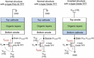
The team demonstrated that using this new material makes it possible to realize organic EL devices that possess performance equivalent to or greater than stacked structures even when using reverse stacked structures. The normal and the reverse stack configurations are illustrated in the figure below.
A great deal of information on the formation and performance of the devices is contained in the article.
The newly developed transparent oxide semiconductors are all reported as transparent and chemically stable. At ambient temperatures, the semiconductors can be formed on a large area. Furthermore, the thin film so formed is amorphous and the surface is, therefore, physically quite smooth. Simultaneous wet etch processing is possible for the thin films which have been formed on the ITO electrode. This makes it possible to construct a process which is well suited for mass production and has the potential to lower manufacturing cost. –Arthur Berman
Tokyo Institute of Technology, Hideo Hosono, [email protected]

