Yesterday, I looked at microdisplays (When is a microLED not a microLED? Part 1) and decided that a good limit to the definition is that the largest side should be 100 microns or less. That set the lower limit for miniLEDs, which are the next category, but the category also needs an upper limit.

Although MiniLEDs are likely to be used in direct small pitch displays, the main application that is being discussed at the moment is the development of direct backlight displays for LCDs. These are being called for to meet two needs. First, LCD makers need to start to compete with OLEDs in providing deep blacks which are very popular for TV and automotive applications, in particular. In automotive, the idea of using a lot of miniLEDs to give deep blacks solves two problems for auto makers.
- The deep black mean that the panels can disappear into the background and the typical rectangular shape of displays is not obvious when the display is powered on, which can happen in the dark with conventional backlights. Auto designers don’t like the look of rectangular displays. It also means that you can use dual displays side by side rather than a single extra wide display. That may be cheaper and allow redundancy.
- OLEDs can provide the deep blacks, but it remains a challenge to qualify OLEDs for automotive use. Audi has put OLED displays to replace rear view mirrors in its new e-tron SUV, but mirrors will only have static images on the display for short periods of time as the mirror is adjusted. On the other hand in the instrument cluster display or central display, there is often static content that can cause image sticking on OLEDs, especially at the higher temperatures seen in some markets.
Moving to the well understood and more easily qualified LCD technology with miniLEDs are a good possible solution.
In TV, OLED has very impressive black levels, but struggles to create high peak brightness and good saturation at high brightness. Large OLEDs for TVs are also only available from LG Display, which makes it hard to haggle and difficult for some TV set makers (well, for Samsung, anyway). At CES, in its private Innovation Room, Samsung showed a TV using the latest version of its VA LCD technology (which improves the viewing angle performance) with a backlight with thousands of zones. It was shown side-by-side with an LG OLED and at the time it was only the second time that, at the same price, I would have bought the LCD rather than the OLED (the first was the Eizo HDR monitor shown at IBC alongside a Sony BVM OLED monitor at IBC in September 2017). There was little or no haloing from the backlight and the peak brightness and colour volume were truly impressive.
Now both of these applications need very large numbers of miniLEDs. Given that LEDs are semiconductors cut from wafers, that means that to keep costs anywhere near feasible for this kind of application, the LEDs have to be very small. If they are too big, you simply can’t get enough out of a wafer to get the price low enough. That suggests that we choose the smallest size that reasonably differentiates from microLED as the maximum size. Most LEDs (and I’m no expert!) are made on 4″ wafers. Based on a ‘back of the envelope’ calculation, a 4″ wafer might produce 20,000 to 30,000 miniLEDs if they are 0.5mm square. However, going down to 0.2mm might mean you could make six or seven times more.
So, it seems to me that while some are talking of as large as 0.5mm as a reasonable size for miniLED, for me that is much too big. The LEDs would just be too expensive for the kind of application that is being developed.IHS Markit has already said that, at current prices, miniLED LCDs will be too expensive.
On that basis, I’m going for a definition of microLED as ‘up to 100 micron’ per side and with miniLED as having a maximum side length of 100 microns to 200 microns.
It seems, in this I’m not alone. In researching this article, I came across the very nice graphic below from Eric Virey at Yole Développement, presented this summer. I also noted that specialist blog, LED Inside is using 200 microns as an upper size for miniLED. It also considers a limit down to 50 microns for the lower limit betwen miniLED and microLED. A key difference that is highlighted by Yole is that while MiniLED can be packaged as SMDs or Chip on Board (CoB) devices, microLEDs are strictly CoB architecture, where the LED chip is directly connected to the circuit board.
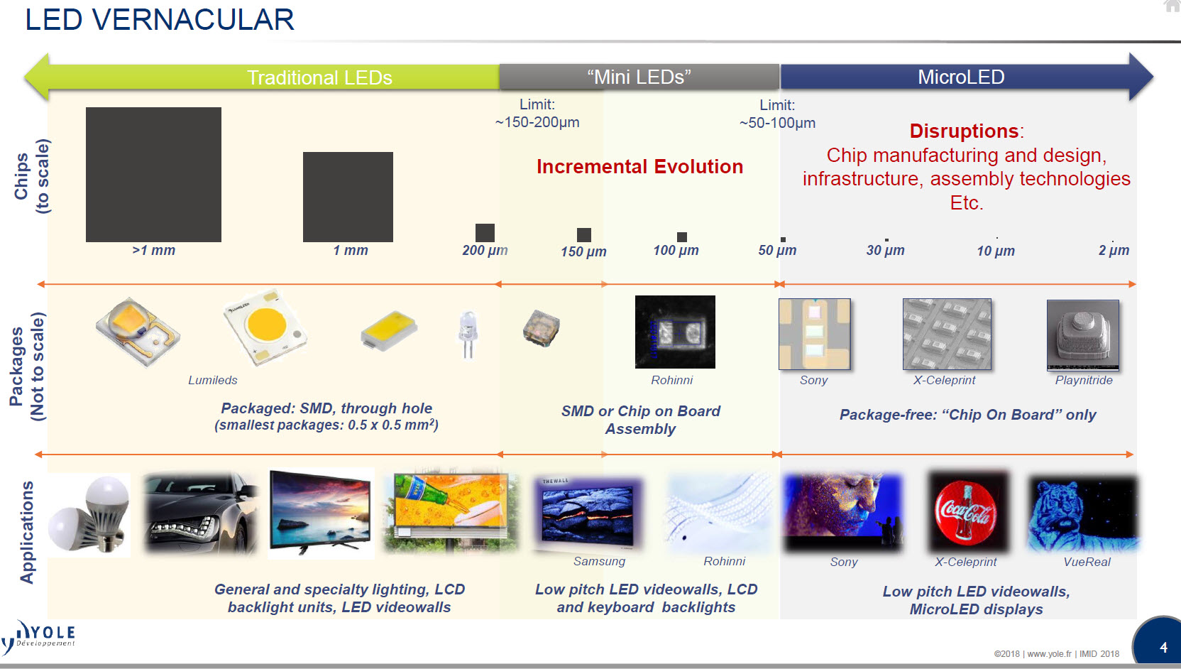 Yole MicroLED Chart – Click for higher resolution
The other alternative would be to work on area as a parameter rather than side length. That would mean that our definition of microLED would be smaller than 0.01mm² while a miniLED would be from 0.01mm² to 0.04mm² of area. (BR)