We don’t get a lot of comments about the topics chosen by our writers on Display Daily. However, recently I got a mail from a reader who asked “Why don’t you do an article about the definition of mini and microLEDs?”.

LEDs, historically, have been pretty big chips. The first LED displays used individual LEDs in red, green and blue. Each LED chip was encapsulated in a separate housing with connections and an optical element. The size of the LEDs meant that the pixels couldn’t be very close together (20mm or so was quite typical) – in 2000 we reported on a breakthrough by Lighthouse in getting from 10mm to as small as 5mm pitch!
If the pixels are far apart, the image looks poor if it is viewed from too close a distance. There used to be a rule of thumb that you should allow at least a metre of viewing distance for each millimetre of pixel pitch. I would suggest the reality is that 1.5m or more is really ideal. If you were making an LED display in those days with a pitch of, perhaps, 20mm, you wouldn’t want to view it from less than 20 metres. That meant that most of the displays using this technology were installed outside or only in very large spaces and viewed from far away.
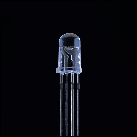 Tri Color LEDs were originally made to look like regular individual LEDs.
To improve things, LED device packagers started to take the three individual LED chips and put them altogether in a single package that could produce any combination of RGB. That kind of architecture is the basis of all the small pitch LEDs that are increasingly ubiquitous in public places and look good even when viewed from relatively close up. Originally, these were made to look like individual LCDs, with lenses, but then the design changed to allow the LEDs to be surface mounted on the PCB (SMD architecture).
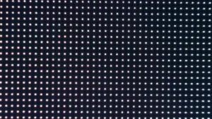
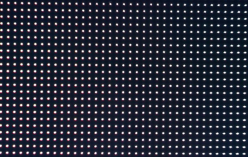
You can keep making the LED packages smaller and smaller to make the pitch of the finished display smaller and smaller. These days, the “State of the Art” of this kind of display is at around 0.9mm.
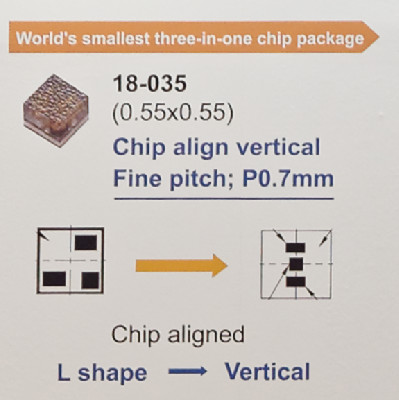 Everlight showed this SMD display chip at Electronica in 2016. Image:Meko
Things start to get tricky at that size because of the need to dissipate heat and power and the brightness of this kind of display is quite a bit lower for most of these displays, although vendors such as Silicon Core have done better than others and are able to use different architectures and driving methods to stand out from the crowd.
Sony really put the cat among the display pigeons at CinemaCon and Infocomm in 2016 by showing its Crystal LED technology. This technology changed things by making the chip devices very small and surrounding the small LEDs with large areas that were black. That gave better black levels than traditional approaches could achieve. Sony took the LED chips and mounted them directly onto circuit boards, a technology known as ‘Chip on Board’ or CoB. Others have also been trying to develop the same concept with more or less success. Chip on board has some challenges, although Sony has done a good job – albeit at a price that’s in the realm of ‘if you have to ask the price, you can’t afford it’.
 I got this close-up shot of the Sony CrystalLED at Infocomm 2016. The small LEDs and big black area are very clear. Image:Meko
However, what Sony did with this display is to show how good LED could look. The viewing angle issues are very small as the LEDs are emissive and there are no issues of speed, while colour gamuts can be wide while lifetimes are very long indeed. So this is a technology worth pursuing. Further, LEDs are one of the most efficient ways of converting electrons to photons with the environmental advantages that brings.
Now, Sony had previously shown the same concept as a TV back in 2012 when it showed a 55″ FullHD TV demonstration at CES. It looked very good and the rumours were that it had been made over a period of several months, by hand! That is to say the six million or so LEDs were individually placed. Sony showed it just as a technology demonstration and hasn’t so far commercialised anything this small.
So, as far as we are concerned, the kind of size that Sony used is a microLED and for many the definition is a size of less than 100 microns (0.1 mm) along the edge. Samsung, as is its way (with LED displays for LCDs with OLED backlights, for example) decided to use its own definition for the term microLED and describes its ‘Wall’ display as having microLEDs, although they are around 0.4mm x 0.125 as far as we can tell (see below), so they fall outside our definition.
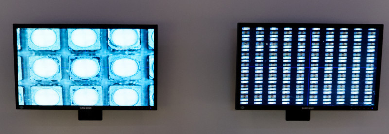 Samsung showed these microscope images at CES. Convnetional LEDs are on the left and its ‘Wall’ 146″ TV is on the right. Image:Meko
 This better image of the Samsung Wall display shows that the LEDs are much bigger than on the Sony CrystalLED. Image:Meko
Samsung describes its Wall LED display, shown at CES this year, as being made of microLEDs, but it showed a microscopic image of the display at its press event. The pitch of the display is 0.82mm (calculated from the diagonal and resolution). That means that the LEDs in the picture are 410?m x 124?m by our calculations from the image we took. They are very different from the Sony pixels. Sony quotes the area of the pixels on its display as having an area of less than 0.003mm² which would mean that each side (assuming they are square) is 54 microns, so it fits our definition of microLED. The Samsung LEDs, on the other hand, would be 0.051mm² – some 17 times larger than the Sony device.
Now, the lower size of miniLEDs is effectively set by the upper end of the microLED definition, but it is less clear where the upper size limit should be. I’ll look at that tomorrow and there will be a link to the article below, when it is published. (BR)