One of the more interesting presentations at the recent Display Summit (proceedings available soon), was a paper from Vladimir Matias at iBeam Materials. His company works closely with Sandia National Labs where they exploited thin metal foil technology used for superconductors to develop a novel microLED approach called GaN-on-Metal.

This could be quite a breakthrough in LED/microLED fabrication as it may transform how LEDs are made and used.
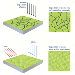
The key is an ion-beam processed crystal alignment layer that sits between the metal foil and the epitaxial growth layer of GaN. The process is shown below.
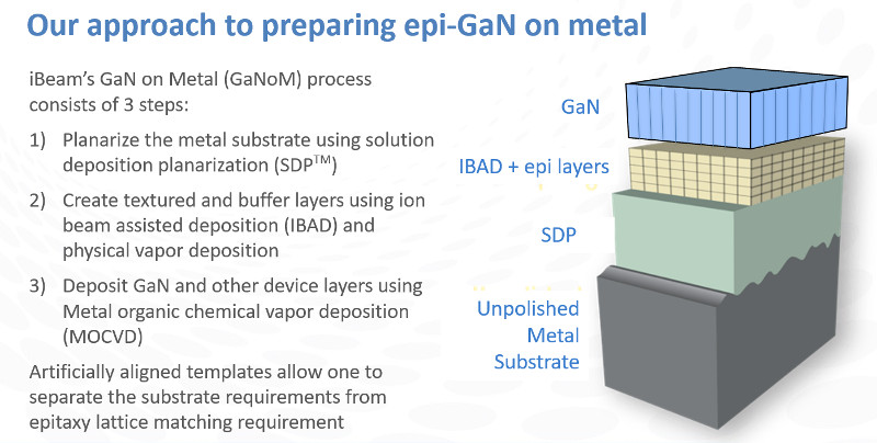
The Ion Beam Assisted Deposition (IBAD) process is used to align the grains in the epi layers to create a single-crystal-like layer for MOCVD GaN growth. Matias says the process is extremely fast aligning the grains in 1 second with a less than 5nm epi layer.
Key benefits include a much improved heat sink for lower device temperatures, better wavelength uniformity so no binning needed, plus the metal foil is a natural reflector for better light extraction. The first blue LEDs have demonstrated a 70% IQE from photoluminescence. LED devices as small as 10 microns have been fabricated and a bend radius of 7mm is possible too.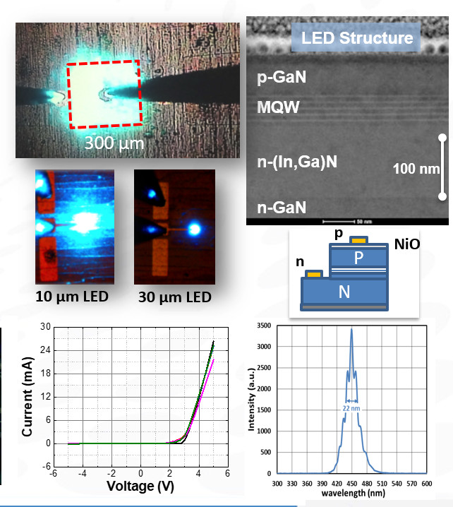
What’s really cool is that this now creates the possibility of making GaN devices in a roll to roll process on metal foil. This could revolutionize not only microLED fabrication, but could also be used for LEDs for all kinds of applications. Think flexible LED displays.
While it still early to be forecasting the cost of production, Matias thinks this R2R process can be much less expensive than planetary deposition systems used in GaN wafer fabrication today. The cost per area depends heavily on the width of the R2R web tool, but his model suggests GaN deposition costs of $0.32 per cm² for a 10cm wide web and a mere $0.07 per cm² for a 100cm wide web. That would make it cost competitive for a microLED cellphone display compared to OLED.
MicroLED devices can be made directly on this GaN substrate as transistors and emitters can both be made with the materials. Black photoresist would cover these parts while patterning of quantum dots would be needed for red and green. A color gamut in excess of DCI-P3 has already been shown.
If this can be commercialized, it may offer a path for low cost pixels at high density – exactly what is needed for light field displays. – CC