AMD has announced a new GPU architecture called Vega that is for PC gaming, professional design and machine intelligence. AMD said that these applications need fast access to massive amounts of memory. The Vega architecture’s memory subsystem enables GPUs to address very large data sets spread across a mix of memory types. The high-bandwidth cache controller in Vega-based GPUs can access on-package cache and off-package memories in a flexible, programmable fashion using fine-grained data movement, the company claims.
- ‘The world’s most advanced GPU memory architecture’: The Vega architecture enables a new memory hierarchy for GPUs. This new approach comes in the form of a new high-bandwidth cache and its controller. The cache features leading-edge HBM2 technology which is capable of transferring terabytes of data every second, doubling the bandwidth-per-pin over the previous generation HBM technology. HBM2 also enables much greater capacity at less than half the footprint of GDDR5 memory. Vega architecture is optimised for streaming very large datasets and can work with a variety of memory types with up to 512TB of virtual address space.
- Next-generation geometry pipeline: Today’s games and professional applications make use of incredibly complex geometry enabled by the extraordinary increase in the resolutions of data acquisition devices. The hundreds of millions of polygons in any given frame have meshes so dense that there are often many polygons being rendered per pixel. Vega’s next-generation geometry pipeline enables the programmer to extract incredible efficiency in processing this complex geometry, while also delivering more than 200% of the throughput-per-clock over previous Radeon architectures. It also features improved load-balancing with an intelligent workload distributor to deliver consistent performance.
- Next-generation compute engine: At the core of the Vega architecture is a new compute engine built on flexible compute units that can natively process 8-bit, 16-bit, 32-bit or 64-bit operations in each clock cycle. These compute units are optimised to attain significantly higher frequencies than previous generations and their support of variable datatypes makes the architecture highly versatile across workloads, AMD claims.
- Advanced pixel engine: The new Vega pixel engine employs a Draw Stream Binning Rasterizer, designed to improve performance and power efficiency. It allows for “fetch once, shade once” of pixels through the use of a smart on-chip bin cache and early culling of pixels invisible in a final scene. Vega’s pixel engine is now a client of the onboard L2 cache, enabling considerable overhead reduction for graphics workloads which perform frequent read-after-write operations.
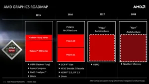
GPU products based on the Vega architecture are expected to ship in the first half of 2017.
For more, see the video on the Vega microsite.