OLED microdisplays researched and developed at the Dresden Fraunhofer Institute for Organic Electronics, Electron Beam and Plasma Technology FEP have already been offered for several years as evaluation kits for potential exploitation partners. In addition to the design of application- and customer-specific microdisplay chips made possible by means of integrated circuit design, the industry-compatible, standardized manufacturing process technology development up to testing and characterization methods plays an important role.
Large-volume applications of microdisplays were in the past mainly limited to electronic viewfinders and projectors (2020 approx. $2 million total sales of microdisplay modules). Especially since the emergence of consumer-ready virtual- and assisted-reality glasses as well as first professional applications of augmented-reality glasses, the microdisplay market is increasingly shifting into these areas. While the figures for 2022 are still manageable (display module sales: Augmented Reality (AR) approx. $176 million, Virtual Reality (VR) approx. $420 million), for 2027 around $7.5 billion has been forecasted just for these two applications.
Fraunhofer FEP in Dresden, Germany, has been researching and developing customer- and application-specific OLED microdisplays and sensors based on OLED-on-silicon technology for years and has also been able to reliably offer corresponding evaluation kits for testing and development purposes to industrial partners. Now the scientists at the institute, especially technologists and IC designers, have optimized the device designs and manufacturing processes for their ultra-low power OLED microdisplays, which are particularly relevant in wearables (e. g. sports glasses, motorcycle helmets), in such a way that industrial manufacturing environments can be verified under comparable conditions. From this stage, there are now advanced opportunities for transfer to industrial customers, e. g. through design/process transfer and licensing for customers’ own products, or pilot manufacturing at medium volumes for microdisplay devices that are not available elsewhere in the market.
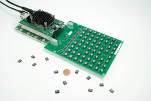
Martin Rolle, engineer in IC and system design, explains: “We have been able to significantly expand and optimize our pilot-fabrication processes in the cleanroom and with our external partners in recent years. Pilot-fabrication capability also includes test regimes and the characterization of components. Here, standardized test regimes now help us to quickly develop and establish customized microdisplays for our customers (e.g. specific color or brightness requirements). Part of this is a new test board, equipped with 64 microdisplay chips each for initial evaluation.”
At embedded world 2023, the scientists will not only show the range of microdisplays and sensors, but also this new test board. “Compared to individual evaluation kits, this offer is intended to support new development ideas and their rapid implementation at start-up’s, SME or large enterprises,” Martin Rolle continues.
The new Fraunhofer FEP test boards also serve to simplify and secure the transport of displays to the customer, who thus has the option of testing up to 64 microdisplays on the test board directly via the corresponding control electronics. This control is carried out by means of an SPI interface (FPGA-based) as standard, but can also be realized via customer’s own solution or customer-specific electronics developed by Fraunhofer FEP and its partners. For this purpose, too, a strong network is already available for our customers through many years of joint projects.

