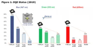
DisplayWeek had many papers and exhibits extolling the benefits of MicroLEDs, which all begin with the extraordinary EQE for 100 µm LEDs ranging from 75% for blue to 45% for red and 40% for green.

The EQE drops as the die size shrinks, such that at 5µm, the EQE’s are 25% for blue, 15% for green and 7% for red. While OLEDs are more efficient for red and green, there is a wide disparity for blue, as shown in the next figure.
 EQE Status – Source:Yole
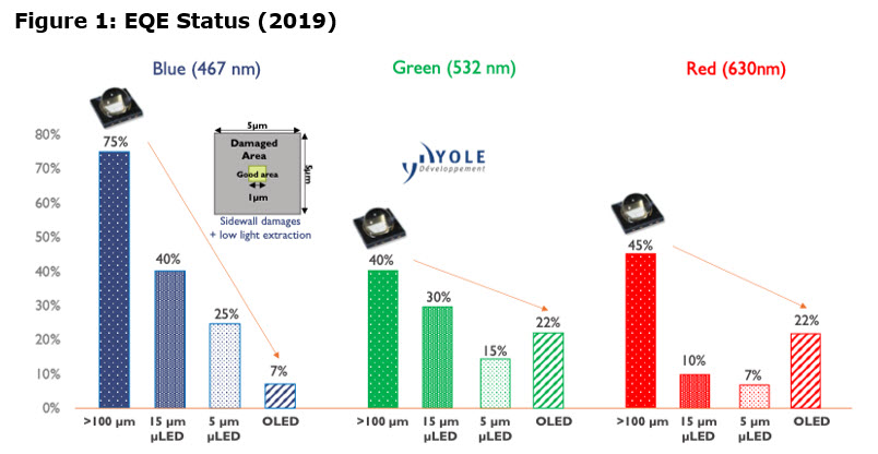
The development of a phosphorescent blue with an EQE of 10-15% is on the horizon and both UDC and Samsung expect a high efficacy blue emitter to reach the market by 2024. However, the performance will still be ½ the EQE of a 5µm blue LED. Also at DisplayWeek, a number of papers discussed potential EQE improvements of 50% by enhancing the OLED stack with the plasmonic effect of replacing the cathode with ultra-thin Ag w/nanoparticles. Such an increase would put a new blue material’s EQE at 15% to 22%, comparable to µLEDs while the red and green at 33% would more than double µLED performance.
The development of Plasmon Outcoupling is still in the labs and years away from mass production, but so are µLEDs with their challenges in mass transport and red efficacy. The papers take a deep dive into the causes that limit the EQE of OLEDs:
- Generated photons in a device are lost to the contact metal due to excitation of plasmons that do not radiate—the effect can be reduced by thickening the electron transporting layer (ETL)
- Emitted light total-internally reflected from a glass substrate—this can be reduced by using a microlens array or light scattering structures in the substrate.
- Light trapped in a device in the form of guided mode due to the device layers serving as waveguide, which is the hardest to extract, because the guided mode formed within the active region including the transparent anode is inherent and propagates along these layers. When sufficiently thick layer of transparent conductive oxides (TCO) as an anode is needed to ensure low film resistivity, it aggravates the waveguide effect.
Efforts to extract the waveguide mode, by patterning or using a grid structure, not only increase the fabrication complexity and cost, but also can protrude into organic layers or result in non-planar surfaces, negatively affecting the surface smoothness important for OLED and its operation lifetime. However, increasing the plasmonic effect by using ultra-thin Ag w/nanoparticles in the cathode (replacing ITO) to eliminate the waveguide mode does not add fabrication cost or affect other properties of the OLEDs.
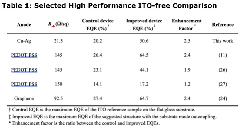
Nick Thompson and members of the UDC staff presented a paper at DisplayWeek 2022, on the effect of Plasmon Outcoupling Efficiency as did Menke and colleagues from the University of Michigan. They reported that their results of extracting energy from the plasmon mode could double the efficiency of PHOLEDs, while increasing device stability by an order of magnitude. The choice of material for an Ag adhesion layer affects the device performance of plasmonic PHOLEDs by incorporating a nanoparticle-based plasmon out-coupling scheme. The next table shows that the efficiency improvement due to enhanced plasmon out-coupling efficiency enabled by improved Ag quality from the adhesion layer.
 Source:UDC
The plasmonic PHOLED couples excited state energy to the plasmon mode of a nearby metal contact to reduce the excited state lifetime, which then reduces the steady state triplet density and the likelihood of destabilizing excited state interactions. Additionally, a nanoparticle-based out-coupling scheme could increase efficiency gains alongside the stability boost, purely through device design, rather than materials design. The material properties of the plasmonically-active metal contact, typically Ag, play a crucial role in determining the efficiency of plasmon conversion to free-space photons. Having two different Ag adhesion layers leads to even further gains in the device efficiency of this plasmonic PHOLED technology. The efficiency improvements shown in the next table are provided by adhesion layer #1 and is related to either the plasmon in-coupling efficiency or the plasmon out-coupling efficiency.
 Source: UDC
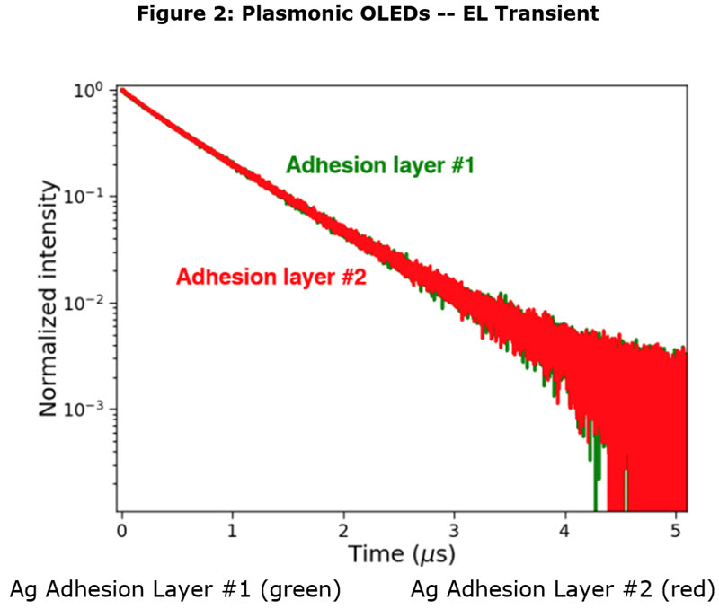
The electroluminescent (EL) transient of both devices was measured and are shown in the next figure. The overlapping decay curves show that the transients are similar, and subsequent modeling with a monoexponential fit yields transient lifetimes of 0.63 µs for both adhesion layers #1 and #2.
OLED design as the momentum matching condition between surface plasmon polaritons and freespace photons means that energy coupled to the surface plasmon mode typically cannot be recovered as light. However, plasmonic PHOLEDs designed specifically to maximize coupling of energy to the plasmon mode increase both device stability and efficiency when incorporating a nanoparticle-based out-coupling scheme.
A critical component of this out-coupling scheme is the quality of the Ag cathode, which determines the plasmon out-coupling efficiency. Silver thin films are frequently used in plasmonics investigations, though the tendency of Ag to form growth islands when evaporated on common substrates, such as glass and organics, necessitates the use of a thin adhesion layer to improve wetting.
 Source:UDC
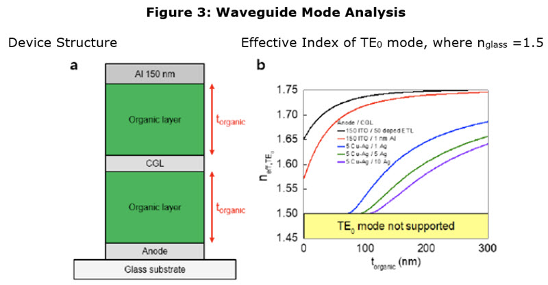
The cut-off thickness for guided mode elimination when using thin Ag as electrode suggests the mechanism will disappear when the organic layers become too thick; therefore tandem OLEDs will still have to face waveguiding problems. But tandem OLEDs can also eliminate the waveguide mode by inserting an ultrathin metal layer in the charge-generation layer (CGL) layer. In theory, the waveguide mode can also be suppressed even in a tandem device as long as sufficient thickness of Ag film is inserted in the device.
The waveguide mode cut-off condition in tandem OLED structures was calculated and compared to the conventional ITO-based tandem OLED vs Cu-Ag based tandem OLED. An ultrathin Ag based CGL was compared with the conventional CGL of 50 nm Li doped ETL and ultrathin metal films. The next figure shows a calculated tandem OLED structure (a) while (b) shows effective index of fundamental waveguide mode, TE0 mode. TM mode is not supported when TE mode is cutoff. CGL can be 50 nm alkali doped ETL material or 1 nm Al layer for the reference tandem OLED. The (b) figure shows tandem OLEDs with ITO anode (reference) excites the waveguide mode along the entire organic layer thickness, meaning that the significant amount of light is trapped inside the device that lowers EQE. However, Cu-Ag based tandem OLEDs show cut-off behaviors at about 100 nm organic layer thickness, which means that Cu-Ag tandem OLED does not have trapped light and can increase device EQE in the end.
 Source:UDC
Most conventional analysis predicts that µLED displays will be brighter, use less power and last longer than OLEDs because of their higher EQE and predict they are the ultimate long-term display solution even if they cost more than OLEDs. But Plasmon Outcoupling could challenge the thesis and offer a lower cost, higher performing option. (BY)
Barry Young is the CEO of the OLED Association
Source: 21-3 / N. J. Thompson Effect of Ag Adhesion Layer on Plasmon Outcoupling Efficiency Nicholas J. Thompson, Michael A. Fusella, Renata Saramak, Hari…
Terms matched: 1 – Score: 160 – 29 Apr 2022 – URL: 21-3.pdf
21-2 / Improve OLED Light Outcoupling Efficiency by Eliminating Waveguide Mode using Ultrathin Metal Electrode Changyeong Jeong, Yong-Bum Park, and L. Jay Guo* Electrical Engineering and Computer Science, University of Michigan, Ann Arbor, MI, USA