Holst Centre Shows Next Step Towards Cheaper Flexible Electronics
by Artem Alekseenko
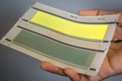
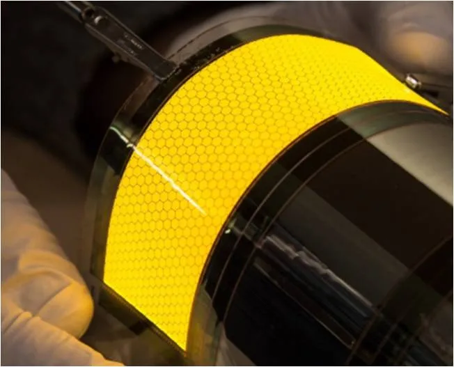
Researchers from Holst Centre have become the first to use spatial atomic layer deposition (sALD) to create both the semiconductor and dielectric layer in a thin-film transistor (TFT) backplane. Using a low-temperature, large-area process …
Tags:Holst Centre


