The Interuniversity MicroElectronics Center, better known as Imec, is a research institution headquartered in Leuven, Belgium that has a lot of interests in OLED and display technologies and with worldwide reach.
![]()
This reach includes Imec International (a legal entity set up under Belgian law), Imec Belgium (supported by the Flemish Government), Imec the Netherlands (including the Holst Centre which is supported by the Dutch Government), Imec Taiwan (ImecTaiwan Co.), Imec China (Imec Microelectronics Shanghai Co. Ltd.), Imec India (Imec India Private Limited in Bangalore) and Imec USA (Imec Inc. headquartered in San Francisco). The Holst Centre is an independent R&D center that was set up in 2005 by Imec and TNO. It is located on the High Tech Campus in Eindhoven and was named after Gilles Holst, the first director of Philips Research.
Imec Florida is the latest addition to Imec USA and was organized in July, 2016. Imec Florida is a collaboration between Imec USA, the University of Central Florida (UCF), Osceola County and the International Consortium for Advanced Manufacturing Research (ICAMR), which was initially funded in March, 2015. Imec Florida is setting up fab facilities for the development and production of III-V-on-silicon solutions for a broad range of applications including sensors, high-speed electronics and photonics. Initially Imec Florida is expected to focus on sensor technology, not displays.
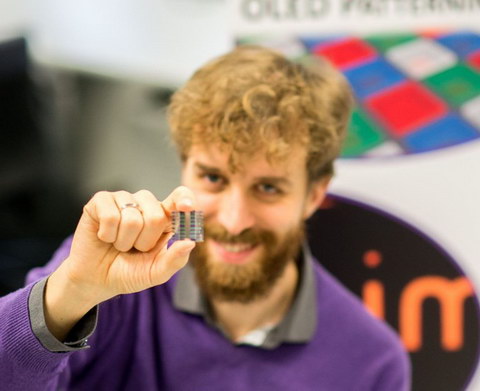 Dr. Pawel Malinowski after winning the IDW 2014 Best Paper Award.
Imec was barely on my radar screen when I ran into Dr. Hanne Degans, press officer and communications specialist for Imec at a recent Pepcom event. I asked her about Imec activities in the display field, including OLEDs, and she put me in touch with Dr. Pawel Malinowski, Senior Researcher at Imec in Leuven working in the Thin-Film Electronics (TFEL) group. He received his PhD from the University of Leuven in 2011. He has published multiple papers on thin-film electronics including OLEDs. For example, he was lead author of paper 74-3 at SID 2016 titled “Multicolor 1250 ppi OLED arrays Patterned by Photolithography.” His 11 co-authors came from both Imec and Fujifilm in both Belgium and Japan. Two of the co-authors are associated with both Imec and the University of Leuven. Another example of a Imec/industrial cooperation was the exhibition of a flexible OLED display in the Touch Taiwan conference in September, 2016 that was a joint development of Imec, the Holst Centre and Chunghwa Picture Tubes (CPT).
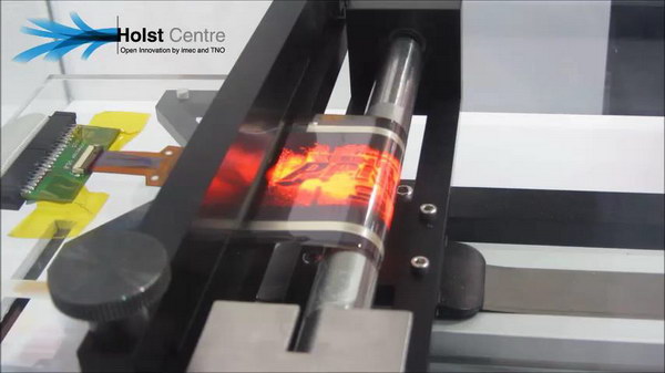 Rollable OLED display demonstrated at Touch Taiwan 2015 in the CPT Booth.
As can be seen from the brief description of Imec and Dr. Malinowski’s work, collaboration, cooperation, joint projects and partnerships are the rule for Imec. This collaboration includes not only universities and other public institutions but also private corporations such as Fujifilm and CPT. Funding for Imec comes from a variety of sources, including both corporations and government entities such as the EU; the government of Flanders, Belgium; and, in the case of Imec Florida, Osceola County. Overall, Imec has about 600 partners.
Due to the highly proprietary nature of display process development, Dr. Malinowski says Imec and TFEL normally work with only a single industrial partner when doing display work. Other Imec projects often involve multiple industrial and institutional partners.
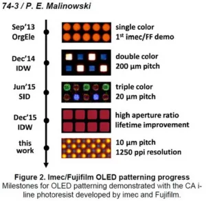
The figure shows progress 2013 – 2016 in the Imec/Fujifilm OLED patterning project. Note the 2016 1250 ppi result was a two-color OLED with red and blue pixels. These are red and blue OLED materials, not white OLEDs with color filters. Future work will include 1250 ppi full color displays suited for UHD-TV and VR applications. In the longer term, Imec expects to integrate sensors in the displays, especially useful for AR and VR applications, and develop holographic displays.
Of the approximately 3500 people at Imec Leuven and 200 people at the Holst Centre, Dr. Malinowski says the TFEL program where he works has about 40 – 50 people in it and is only a small part of Imec overall. In addition to flexible OLED displays, these 40 – 50 people also work on thin film sensors and other large area flexible thin film systems.
Trips to Eindhoven
He and his colleagues in Leuven work closely with their colleagues at the Holst Centre in Eindhoven and he spends part of his time in Eindhoven. The Holst Centre has a complete Gen 1 fab and can work on displays up to 350mm x 320mm. This fab can make a complete flexible OLED display from the backplane through the encapsulation process. While the Gen 1 fab is intended primarily for R&D, it can also do low-volume production in the 100 – 10,000 components range. While Imec cannot demonstrate scaling of technologies developed on the Gen-1 fab to larger sizes, Dr. Malinowski says that scaling is always considered in the process development. Scaling beyond Gen-1 is normally done by the industrial partner (or its other partners), not by Imec.
The key to long lifetime for flexible OLEDs are flexible barriers to keep water and oxygen away from the OLEDs. The TFEL group at Imec has developed a proprietary organic/inorganic/organic stack that allows OLEDs to pass 60C/90RH accelerated lifetime test and provides 2000 hours with zero black spots in the OLEDs. I recently wrote an article titled KAIST and Long-Life, Flexible OLED Displays. (Subscription required) Dr. Choi and his colleagues at KAIST are working on similar layered and flexible barriers but they only claim (at least publicly to date) a lifetime of 720 hours. Imec has also developed new driving schemes for OLED displays. These schemes involve pixel-level OLED current sensors and allow compensation of non-uniformities and degradation, while reducing the power consumption of the display.
The Gen-1 fab at the Holst Centre is also used for large area sensors. One example was x-ray detectors to replace film in a project with Philips Medical. Hyperspectral sensors that record more than three primary colors (e.g. a red, green, blue and IR sensor) have also been developed. Thin film sensors have been made both on flexible and rigid CMOS substrates.
Dr. Malinowski says that, in general, Imec does not develop the advanced materials used in the TFEL program. These materials are normally developed by its industrial partners such as Fujifilm. Imec develops the processes and integrates multiple new materials into a single process. This development process is, of course, iterative. One of the outputs of a process development step is to let Imec’s partner know how the material can be improved for the next series of developmental tests.
 A flexible OLED from Imec and the Holst Centre.
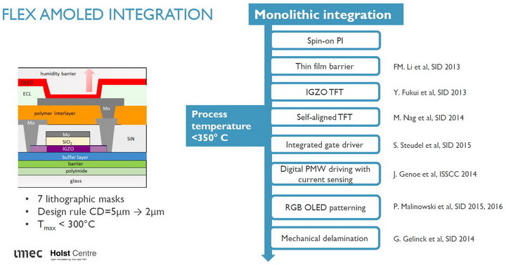
The figure shows a flexible OLED developed by Imec and the Holst Center. Obviously, the device as shown is not flexible since it is still on the glass substrate used during manufacturing. Mechanical delamination of the flexible display from the glass substrate is important, and Imec has developed both mechanical and laser-assisted de-bonding processes. Since de-bonding is less of a problem when you use lower process temperatures, Imec has also developed reliable oxide TFTs that require reduced processing temperatures.
Besides flexible OLEDs, Dr. Malinowski told me that the TFEL group has worked on thin films for other display applications. This includes flexible backplane development using organic or oxide TFTs and integrated, flexible, display drivers.
In his SID 2016 paper, Dr. Malinowski showed a figure on the pixel pitch for 4K and 8K OLED displays. For an 8K 0.5” (12.7mm) microdisplay targeting the VR/AR HMD market, a pitch of >15Kppi is needed with a pitch of <2µm. One of my objections is to VR HMDs is the pixels are normally clearly visible. When (and if) Imec achieves this resolution and pixel pitch, this objection to VR HMDs will go away. He gave no estimated time scale for this 8K development. –Matthew Brennesholtz