IMEC, Holst Centre and Chunghwa Picture Tubes Ltd. (CPT) recently demonstrated an ultra-high resolution display made by photolithography patterning of organic light emitting diode (OLED) materials. The results are a proof of principle demonstration that will pave the way to cost-effective manufacturing of fine, side-by-side pixels in OLEDs.
![]()
This technology was demonstrated at the 6th annual International Smart Display and Touch Panel Exhibition, Touch Taiwan, in Taipei, Taiwan ROC, Sep 20 – Sep 22.
High quality displays are at the core of modern, connected society, with mobile screens enabling and enhancing an ever-increasing number of daily appliances. Active-matrix organic light-emitting diode (AMOLED) displays, with discrete light emitting pixels, are steadily growing, not only in market share, but also in achievable resolution, brightness, size and lifetime.
To continue the advancement of this technology, IMEC together with its program partners has been researching a cost-effective manufacturing method for OLED arrays featuring fine pixels. Pushing the pixel density beyond 1000 ppi is a necessary step for implementation of next-generation displays, especially for virtual reality (VR) and augmented reality (AR). High resolution is also needed to properly render complex Chinese-Japanese-Korean (CJK) characters, even in direct view displays such as smartphones.
CPT and IMEC have verified that a novel photolithography process can allow for ultrafine OLED patterns. The proposed technique does not require using fine-metal masks (FMMs) to structure thermally evaporated OLED stacks (“FMM-free”). One of the main challenges when applying standard photolithography is the damage caused to the organic materials by standard photolithography chemicals. To circumvent this issue, IMEC and CPT have used an i-line, chemically amplified photoresist system, jointly developed by IMEC and Fujifilm, in a process flow dedicated to OLED stacks.
Apart from ultra-high resolution, other benefits of photolithography include high aperture ratio, large substrate size compatibility and good yield control. In addition, patterned RGB OLED displays can be much brighter than the OLED displays made by the color-by-white (CBW) technique where an unpatterned white OLED stack is then separated into colors by a color filter array (CFA).
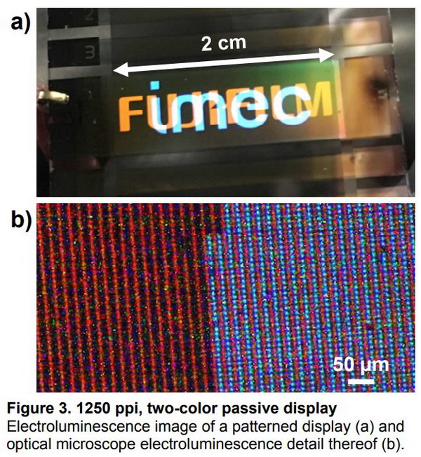
1400 x 1400 passive OLED display shown at Touch Taiwan 2017. The CPT logo is shown in an orange OLED material and the IMEC and Holst Centre logos are shown in a green OLED material. (Photo Credit: IMEC)
The proof-of-concept is a passive display with 1400×1400 pixels (1.96 megapixel) of side-by-side, orange and green OLEDs. The sub-pixel pitch of 20 ?m results in the equivalent resolution of 1250 ppi. Uniform electroluminescence is demonstrated with the possibility of lighting up each color separately. Moreover, preliminary lifetime investigation shows operation of each color after patterning for a few hundred hours at more than 50% of the original brightness.
I wanted more information on this display so I got in touch with Dr. Hanne Degans, press communications manager at IMEC. She passed on my questions to the technical team at IMEC that worked on this display, which included Pawel Malinowski and Tung Huei Ke, who are both researchers in the research group of Prof. Paul Heremans, program director of thin-film electronics at Holst Centre/imec. In a previous Display Daily article on IMEC flexible OLEDs, Pawel Malinowski had provided me with much useful information.
I was told that the initial brightness for the lifetime data was in the range of 300 – 1000 cd/m². When asked about the difference in lifetime between the orange and green OLEDs, I was told by the research team,
“The original lifetimes of the orange and green OLEDs are different. Both pixels can be operated for a few hundred hours at the brightness demonstrated in the prototype. A detailed characterization of each color in a multicolor system is ongoing and is one of the main research topics in our R&D program.”
When I asked about using this OLED patterning technique on a fully-functional backplane, I was told,
“We have demonstrated integration of patterned OLED frontplane on top of imec’s/Holst Centre’s IGZO TFT active matrix flexible backplane – the results are included in our SID 2017 paper. In this way, we can confirm that the photolithography patterning process is compatible with the full process flow of a flexible TFT backplane. This means, that the chemicals, temperatures and equipment used fits in the display process flow.”
The SID paper referred to was an invited paper, number 44.1, titled “Photolithography as Enabler of AMOLED Displays Beyond 1000 ppi.” Pawe? Malinowski was the lead author with 11 co-authors from IMEC, the Holst Centre and Fujifilm. These co-authors included both Tung Huei Ke and Paul Heremans. The Holst Centre contribution was the IGZO backplane on a flexible substrate produced on its Gen-1 TFT pilot line while Fujifilm supplied many of the photolithography materials and IMEC did the patterning and made recommendations to Fujifilm on needed changes in the materials to enable further development.
This paper does provide lifetime data on patterned blue and says the T75 lifetime is above 200 hours for a small molecule, fluorescent blue stack integration with a flexible, IGZO-based active TFT backplane. The paper also says the process is not limited to 20µm sub-pixels and shows images for sub-pixels as small as 3µm. This pixel pitch would small enough to provide a 8466 ppi monochrome display. The paper says it is very difficult to achieve small pixels with fine metal masking (FMM) or inkjet printing (IJP) technology, taking into account issues with yield, uniformity and cost: hence the need for photolithographic patterning of the OLED materials.
 A display similar to the one shown at the CPT booth at Touch Taiwan, with the FUJIFILM logo substituted for the CPT logo. (Image Credit: Society for Information Display 2017 paper 44.1)
Since the demonstration at Touch Taiwan showed only orange and green OLED materials, I also asked whether the same technology could be used to pattern blue OLEDS needed for a full color display? I was told
“We have demonstrated patterning of blue OLEDs in our previous papers (SID, IDW). Actually, our first lifetime results were demonstrated (in) a blue fluorescent stack. In that case, we have published T75 lifetime at 300 nit initial brightness of above 220 h. Right now, we are testing different OLED stacks to improve our process flow.”
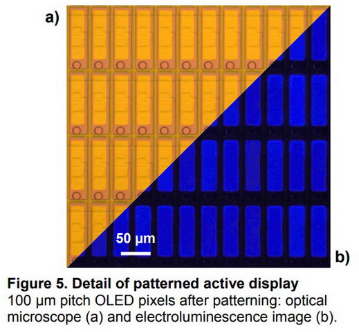 Patterned blue OLED materials (Image Credit: Society for Information Display 2017 paper 44.1)
In conclusion, Paul Heremans stated,
“Our goal is to identify and explore technology bottlenecks in the extremely competitive and fast-paced display industry. With research activities spanning from material and device science, through design, fabrication and integration all the way to tech transfer, we make use of our semiconductor and thin-film background. The collaboration with CPT enables us to improve the manufacturability readiness level of the OLED photolithography patterning method. This will enable production of ultra-high resolution OLED displays for next-generation user interfaces. We are very happy to have the possibility to explore this exciting technology route with our innovative partners.”
-Matthew Brennesholtz
Analyst Comment
Clearly this technology is still in the R&D phase, not pre-production so don’t expect fine-pitch OLEDs from CPT in the near future, at least not made with this process. Still, with both CPT and Fujifilm in the loop, the researchers at IMEC and the Holst Centre are not likely to stray too far from a production-worthy process. Since one of my main complaints about VR is inadequate display resolution, 1250 ppi will be a good step forward. Achieving 8466 ppi in a production display would be more than just a step forward – it would provide all the resolution virtually any AR or VR system would ever need. But just think about the data rates (50 – 100 Gb/S) needed to drive a display like that at the 90FPS needed to put the “Reality” in virtual reality! As Clay Bavor, VP of Virtual Reality at Google, said in his Keynote Speech at SID last May, “Oh Dear!” MB