
TechBlick published extracts from a number of the many speakers that it has lined up for its event next month. There were a number on microLED that we haven’t covered, or not recently so I’ve extracted them for today’s Display Daily.

Holst Centre Developing Laser-Induced Forward Transfer.
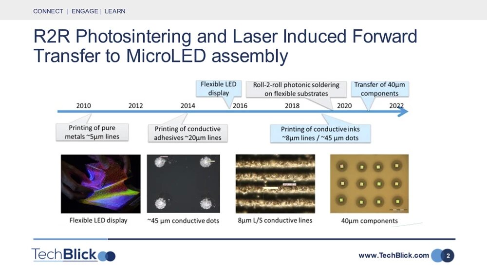
The Holst Centre, an R&D organisation was set up in 2005 in Eindhoven in the Netherlands and we have covered their developments a number of times. In microLED, the institute has developed a number of technologies for microLED. One is Roll-to-Roll photonic soldering on flexible substrates that can accelerate soldering (attachment) of microLEDs onto a substrate. When optimised, it can take place on the scale of milliseconds, much shorter than the timescales of classic reflow for solder or heat curing for electrically conductive adhesives (ECAs).
Of course, one of the challenges of microLEDs is getting the LEDs onto the substrate using mass transfer and that’s where LIFT or Laser Induced Forward Transfer comes in. It offers a way to transfer the microLEDs onto a substrate at speed. Pulses from an ultraviolet (excimer) laser enter through the back of the carrier, which is transparent. The laser light is absorbed in the thin layer of adhesive which has been holding the microLEDs to the temporary carrier and vaporises it. This physically blows the microLEDs off the carrier and pushes them onto the final display panel, which is placed in close contact. Adhesive on the final glass panel holds the microLEDs in place after the transfer. This method allows LEDs made on sapphire to be transferred economically over large areas at high speed.
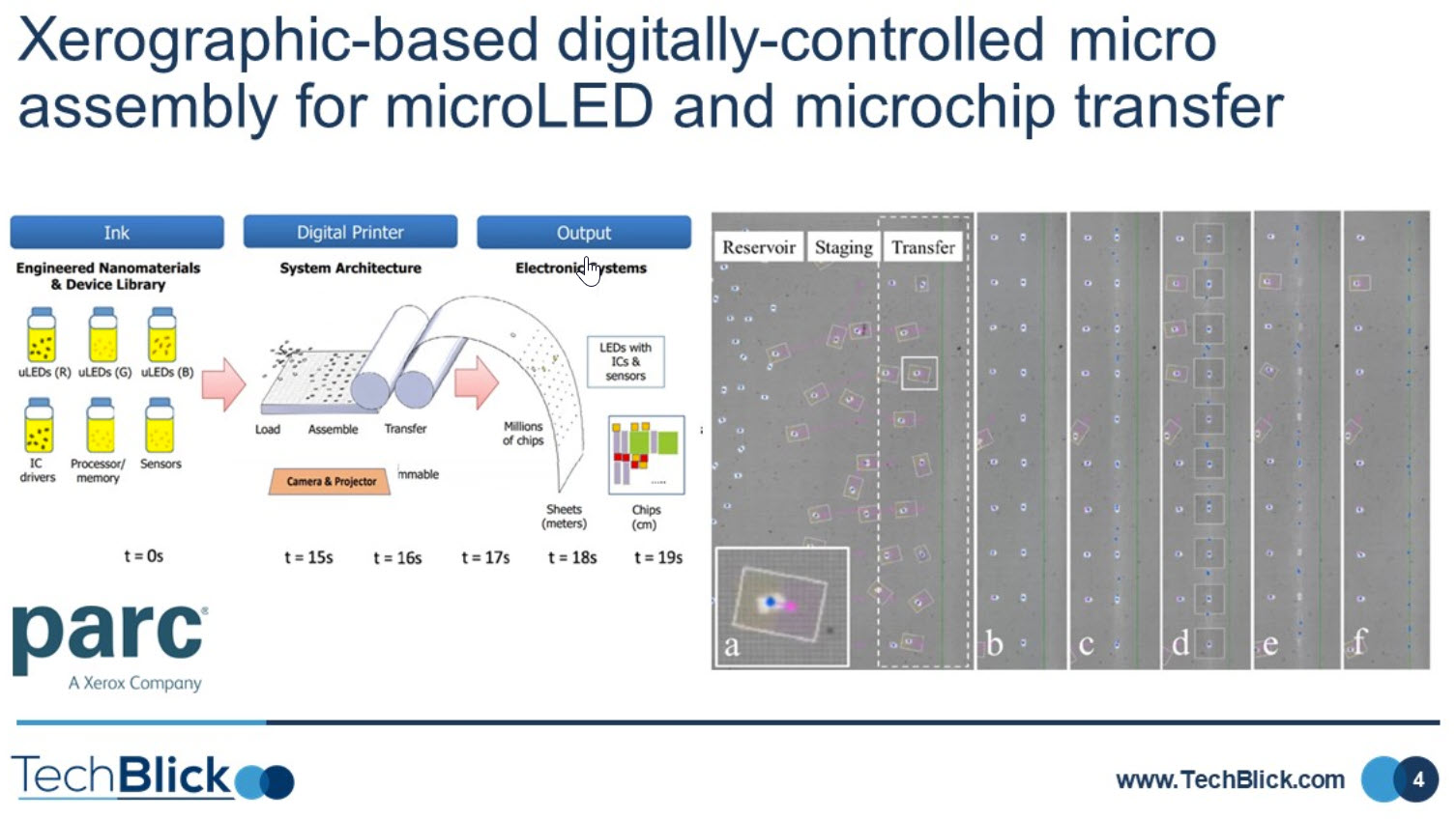
Xerographic-based digitally-controlled micro assembly for microLED and microchip transfer
Another interesting, earlier stage, development is by Parc, a Xerox company. The idea is based upon xerographic printing. Here, microchips such as micro GaN LEDs are suspended in a solution. They are then cast onto an active-matrix substrate controlling a 2D array of electrodes which generate electrostatic force to spatially move the individual chips under the gaze of a camera.
The 2021 demonstrator is still small size (2.5 x 2.5 cm) on 50µm LEDs with no yield data. The assembly process is achieved using a projector addressing a photoswitch array. The assembly process, from mass disordered deposition to liquid to final alignment, is shown below. Currently it is too slow, but an order of magnitude improvement can make it competitive.
The process has interesting development potential as it does not require any special microchip structure. The alignment and positioning is also software controlled, thus allowing arbitrary and complex shapes.
Tape-on-Reel Allows Scaling to Large Displays
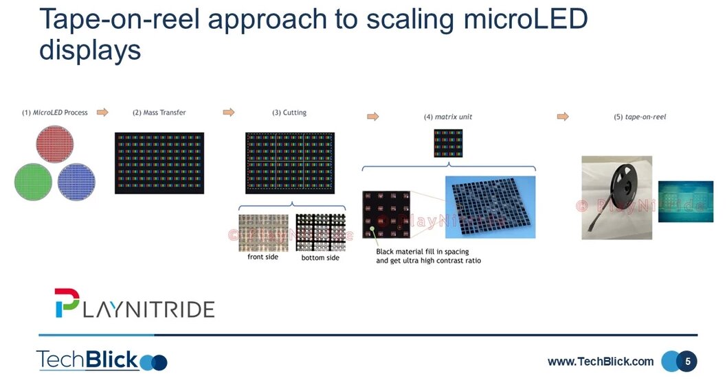
There are a huge range of innovations in the microLED field. Another one that we wish to highlight is in creating a method to assemble large-area microLED displays from tape-on-reel approach. This is a very interesting innovation in the field by PlayNitride, based in Taiwan but reported to be working with AUO, Samsung and Seoul Viosys among others.
The tape-on-reel idea is shown below. Here, the microLEDs are first transferred into a larger panel and are then cut into smaller tiles. The tiles undergo an inspection step and the black filling material is added to enhance contrast. The titles are then added onto a reel, creating a tape-on-reel approach enabling the construction of large microLED displays using a SMT-like process.
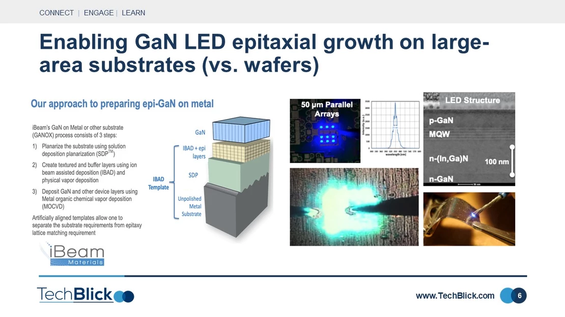
Enabling GaN LED epitaxial growth on large-area substrates (vs. wafers)
Epitaxy is today carried out on rigid single-crystal wafers to make GaN LEDs. This yields high-quality low-defect LED wafers but over limited areas. But what if LEDs could be grown on large-area substrates such as glass or metal foils?
This technology is very interesting, albeit still at a low-tech readiness level. It has a tiny, almost negligible, fraction of the accumulated experience that the wafer-based LED industry has. It is in fact yet to fully assess QY, lifetime, economics and other important factors of GaN LED growth on large-area substrate. Nonetheless, it is a promising approach. (BR)
This article was based on extracts from two more extensive articles published by TechBlick. The items were republished with kind permission.
- The Depth & Breadth Of Innovation In The Display Industry (I)
- The Depth & Breadth Of Innovation In The Display Industry (II)
The articles were promoting TechBlick’s upcoming LIVE(online) interactive conference on Displays & Lighting: Innovations & Market Trends (14-16 July 2021)