A publication from a team at the Institute for the Study of Nanostructured Materials (Bologna, Italy) reports recent developments relating to Organic Light-Emitting Transistors (OLETs). These are a type of organic device that combines the current modulating function of a transistor with light emission. One feature that makes these devices interesting is that they offer the potential for improved efficiency as compared to conventional active matrix/OLED devices.
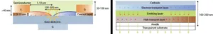
The so-called ambipolar OLET allows transport of both positive (hole) and negative (electron) charges. The ambipolar regime is characterized by hole accumulation next to the source electrode and electron accumulation next to the drain electrode. This is indicated in the illustration of the device structure presented in the left hand figure below. A conventional OLED is illustrated on the right in which the charges move vertically.
The recombination of electron and hole currents moving in-plane is controlled by the gate electrode. The intensity of the electroluminescence can be adjusted by the voltages applied at both the drain and the gate electrodes. It follows that, in the OLET device, the position of the recombination zone can be moved within the transistor channel by varying these applied voltages.
As explained in the article, one advantage inherent in the structure of an OLET device is the potential for higher electroluminescence quantum efficiency. This, in turn, leads to higher efficiencies overall as demonstrated in experimental results published by the team.
In this demonstration, the team constructed an OLET device that was “equivalent” to an OLED. It was found that the optoelectronic characteristics of the OLED device was “typically” exhibiting a maximum external quantum efficiency of ∼0.012%. This value was almost 100 times lower than the corresponding external quantum efficiency of the OLET device. Stated more technically, a “suitably engineered OLET architecture allows for minimizing the exciton-polaron quenching mechanism that leads to reduced external quantum efficiency in OLEDs at high current densities.”
Another determination made by the team is that “implementing OLETs in the design of highly integrated organic optoelectronic systems and innovative pixel architectures requires strict control of the emission area geometry. A 20 – 100μm illuminated area is necessary to develop OLET-based display technology with a favorable ratio between illuminated and dark areas in the pixel.” To address this need, the team demonstrated that “in a suitably optimized OLET architecture, both the position and the extension of the emission area can be controlled by the applied voltage, achieving illumination of the entire transistor channel.”
The article offered the following conclusions:
- Combining electrical switching and light emission in a single device reduces the number of switching thin-film transistors needed in the driving circuit.
- The device architecture is easy to process and naturally avoids pinholes and shorts between injecting contacts.
- The processes used to fabricate OLET devices are well-established, electronic and photonic planar technologies. This, in turn, may ease the way to commercializing OLETs in optical communication and optoelectronic systems.
Looking ahead, the team stated plans to introduce a 1D planar optical cavity as a functional multilayer in the OLET device structure. -Arthur Berman
Institute for the Study of Nanostructured Materials, Stefano Toffanin, +39-051-6398514, [email protected]