
This week I thought we would have two small issues, but Matt contributed an interesting report on the Laser Display and Lighting Conference (which was nearly all displays) and a report on an HDR mastering session in New York by Sony that made LDM much bigger than I expected. However, our MDM issue was thinner than usual as we are ‘head down’ getting our IFA report ready. It will be ready by the middle of next week (and needs to be as we’ll be off to IBC, then!).
Our front page looks at the plans to develop an Oxide TFT, so I thought it would be interesting to look back. We first reported on the new idea of oxide TFTs in 2008 (Display Monitor Vol 15 #13) from the DisplaySearch FPD Conference.
Now, for readers that are not aware of the different kinds of transistor (and at a very crude level), displays are best made with smaller transistors, especially LCDs which are usually transmissive. That means that the transistor blocks some of the area of the pixel, the smaller you make the transistor, the more light that gets transmitted. On the other hand with an OLED, you need more transistors as you need to control the current, so OLEDs also need smaller transistors. The size needed for a transistor basically depends on a metric which is the ‘electron mobility’ of the material used – that is to say, effectively, the ease with which electrons can move through the material.
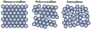
Silicon, like carbon, can existing in different forms. Carbon can be soot, or graphite or diamond. Silicon can be amorphous (like soot), polysilicon (semi-crystalline like graphite) or crystalline (like diamonds). Silicon chips are made from crystal silicon chips. Big LCDs are made with amorphous (a-si) silicon. Wikipedia says the maximum electron mobility (all in cm²/(Vs)) achieved is 1400 for crystal, 100 for polysilicon and approximately 1 for amorphous silicon.
Allotropic forms of silicon – image Wikipedia
Polysilicon is made by depositing a-si and then melting it with a laser. As the silicon cools, it adopts a more crystalline structure. Unfortunately, that is an expensive process, because of the cost and lifetime of the lasers and is difficult, especially as the area of the display increases. (That was one of the roadblocks in Samsung’s plans to make large OLEDs – it wanted to use polysilicon). With big areas, it’s both hard to heat evenly and it’s hard to cool it evenly, so the properties can vary.
Now the idea with oxide TFTs was to replace silicon with other materials, especially indium gallium zinc oxide (IGZo), which, the promise was, could be deposited like a-si, but had properties closer to polysilicon. In 2008, the promise was of 35cm²/Vs. IGZO was developed in Japan and patented by JST and was licensed to Samsung and Sharp in 2011 and 2012, respectively.
However, it has turned out a lot harder to get into volume production than was expected. There was a huge amount of knowledge and understanding of silicon and its processing that was not available for IGZO. I’ll leave it for others to explain the reasons that IGZO has struggled to take over as the dominant technology, although, eventually, it still might. LG, in contrast to Samsung’s use of polysilicon for large OLEDs, adopted IGZO for the substrates for its large OLEDs. However, we hear that the most difficult challenge for LG Display in ramping up its OLED fabs to high yield is the difficulty of making the substrates.
A search of our database shows around 280 articles mentioning IGZO since that first article in 2008 with more than 50 over the last three years. The technology remains an important one for the future of LCD as well as OLEDs.
Bob