Peter Palomaki used to work for QD Vision, but he is now a quantum dot materials consultant. His presentation started with a review of some of the quantum dot architectures along with their strengths and weaknesses but he quickly moved on to discussing the issues with placing quantum dot materials directly in the LED device. This would create white light in the backlight similar to that when using an QD film, but without the film (and presumably at lower cost).
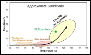
But the optical power density for QD on LED is quite high as shown in the chart.
Palamaki said he was aware of one company Pacific Light Technologies, that has developed prototypes using a Lumileds LED, but it is not commercially available. He then described that the QDs must be embedded in the silicone encapsulant that covers the LED die and that the placement of the QD relative to the LED die can have a big impact on the thermal loading the QDs experience. Theoretically, adding quantum dots to the LED manufacturing process should be simple, but the materials need development. Perhaps a dozen companies are thought to be working on this approach, but little published information is available.
Turning to microLEDs, Palomaki explained that these can be 3 to 100s of microns in size vs. several mm for conventional LEDs. They are fabricated in GaN so you make an array of blue LEDs that must have red and green quantum dots added to them to create a full color microLED.
The advantages of microLEDs include high brightness, lower power, improved efficiency, flexible substrates, semi-transparent and wide color gamut. The challenges are many as the technology is still quite immature. For example, Palomaki estimates the optical flux levels in excess of 60 W/cm² – a significant challenge.
However, quantum dots can solve the color problem here and phosphors are not suitable because a single phosphor particle is μms or tens of microns in size, so might cover multiple microLEDs.
There seems to be quite a bit of activity in microLEDs nonetheless. Devices can be made with two basic approaches. The pick and place scheme uses some method to expand the tight spacing of the microLEDs on the GaN wafer to a bigger pixel pitch. This may be useful for watches, for example. Alternatively, one might define display on the GaN wafer and use this high density in AR or VR applications.
Palomaki concluded by saying he thinks small area microLEDs could be commercialized in the 1-3 year time frame but larger sizes will take longer.