Three additional opening cornerstone presentations at the 2015 Printed Electronics Conference (Santa Clara, CA, November 17-20), provided insight into the nascent but growing pervasiveness of printed electronics. The speakers for the three presentations were from the US Olympic Committee, Hewlett-Packard, and Qualcomm.
Mounir Zok, Senior Sports Technologist for the United States Olympic Committee, presented “Wearable Technology is Changing Sports Forever“. Zok began his presentation noting that in competitive sports athletes need just a small, perhaps 1%, edge to win in their competitive event. Going forward, a key requirement for athletes in training is to measure what is measurable in their performance, and go on to make measureable what is currently not being measured. Zok noted that the many of the technologies being discussed at Printed Electronics 2015 enabled by mobile devices, the internet of things, batteries, sensors and more, have revolutionized his work analyzing athletic activities. He maintains that athletes today are more intelligent and better informed than in the past.
As an example of this trend Zok cited an example involving team pursuit cycling (photo below). He described the approach utilized to define the measurable quantities and the means to measure them, the instrumentation required for the athlete, the bicycle, and the venue, and the atmospheric effects. He went on to describe the use of networked sensors and real time analytics combined with an easy to use “dashboard” to provide insight and information to athletes and coaches. Zok concluded his presentation noting the a key message to companies working in the space, is to bring the right people on board including coaches and athletes, and to consider the users of the instrumentation and data and not focus solely on the technology itself.
 Source: US Olympic Committee
James Stasiak Distinguished Technologist Hewlett-Packard, spoke on “Printing the Future – Building the Trillion Sensor Network One Droplet at a Time“.
Stasiak began his presentation observing that the emerging trillion sensor network is just the next step in the evolution of the information technology. Looking to the future, Stasiak sees a time when every person will own somewhere in the order of 1000 sensors. These sensors will reside in a number of locations and systems ranging from cars, homes and mobile devices to healthcare devices – essentially the internet of things is already here. A further development Stasiak sees as a requirement is to make sensors more situationally aware and to provide for “learning sensors.” To support establishment of the “trillion sensor network”, Stasiak stated that sensor cost must be less than about $0.10 each.
This very low cost sensor requirement means that to realize the “trillion sensor network”, new manufacturing methods will be required to scale to both the production volume and price points needed. As an example, he noted that RFID industry essentially kick-started the internet of things in terms of price and production volume. RFID devices enabled by printed or additive electronics point the way to advanced materials and manufacturing technologies such as functional inks and inkjet printing. The number of developers of materials and manufacturing equipment exhibiting on the Printed Electronics 2015 exhibit floor illustrates the efforts being undertaken to enable the “trillion sensor network”.
Finally, Qualcomm R&D Manager Stein Lundby presented “Creating Surface Electronics for Value-Added Product“. In his talk, Lundby contrasted the current state of conventional electronics emphasizing short switching times, high transistor count and sophisticated, expensive fabrication plants, with a need to develop “surface electronics” with attributes of low cost and large substrate area which make use of longer switching times, flexible substrates and cheaper, simpler fabs. Lundby acknowledges the challenges of such a surface electronics industry including the lack of industry structure, the disparate technologies and technology developers, and challenges for potential customers.
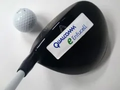
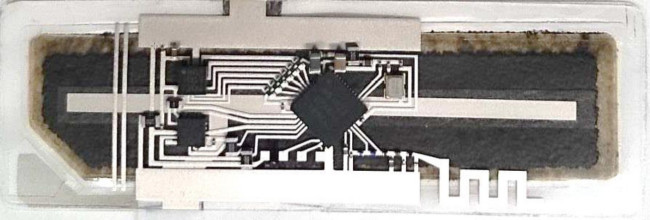
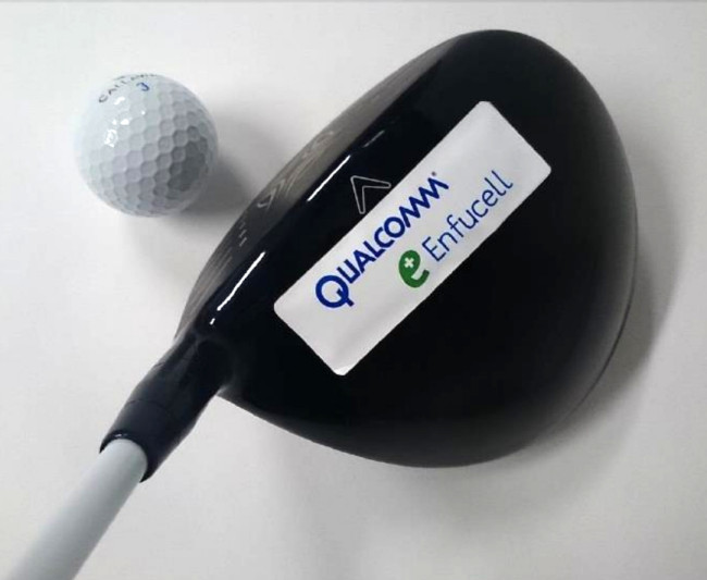
However, Qualcomm is working to enable such an industry (that he calls the “internet of everything”) which will lead to 25 billion connected devices by 2020. Clearly, Qualcomm wants to profit from the evolution of such a large opportunity. To this end, Qualcomm has developed an integrated hybrid electronics sensor platform combining packaged electronic components, conductors, and a battery to form a single monolithic device (photo below top). The design objective of this sensor platform was to incorporate robust components including a 3-axis gyroscope, 3-axis accelerator, which can be low enough cost to be disposable with a 1 hour to 7 day lifetime, and a “Band-Aid like” form factor and application. In a joint development with Enfucell, a printed battery supplier, Qualcomm has demonstrated a golf-related application of its sensor platform (photo below).
 Source: Qualcomm
While Qualcomm acknowledges that there are challenges to the development of such surface electronic products including circuit pattern printing, electrical characteristics including materials performance vs. processability vs. price, rigid board vs. prototype product vs. actual product, mechanical stress, design for mass manufacturability and more, the firm clearly believes that such surface electronic products are right for the market at this time. – Phil Wright