It’s been a few years now since perovskites first came on the scene as a novel material for displays, so I figured an update was due. For those who are unfamiliar, perovskites are a class of materials known for their excellent light-emitting properties. In displays, they could find a home as a down-converter of blue light into red and green, much like the role phosphors and quantum dots play today. In some ways, perovskites are similar to other down-converting materials in that they can very efficiently convert higher energy, blue photons into red and green photons. But in other ways, perovskites are superior. A few examples:
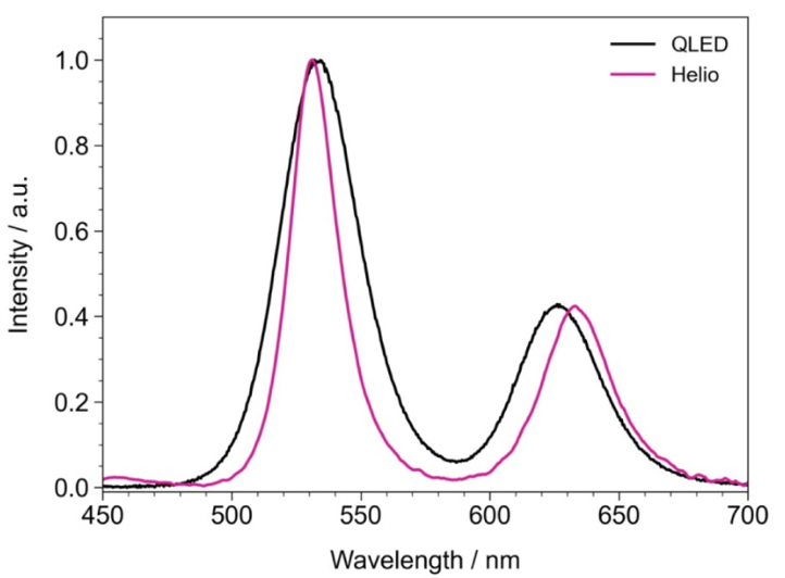
Perovskites (especially green) show ultra-narrow color purity with emission peak widths of 20-25nm. For reference, InP QDs used by Samsung and others are typically in the 35-40 nm range.

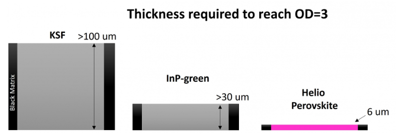
Light absorption of perovskites far and away exceeds all other commercial down-converting materials, phosphor or QD. While QD’s often contain shells that contribute very little to light absorption, perovskites are made of 100% absorbing material, with a high intrinsic ability to absorb blue light. This means that more light can be absorbed in a shorter pathlength – something that is important to color-converted architectures such as QD-OLED.

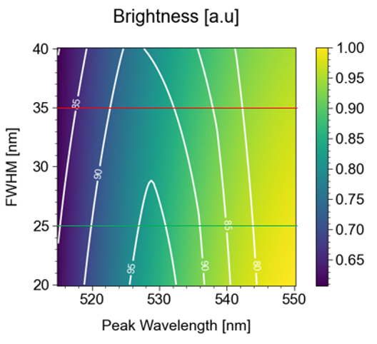
Similar to QDs, the emission wavelength of perovskites can also be tailored to meet the needs of the customer. Recently, perovskite company Helio Display Materials presented a paper summarizing some modeling work they have done to optimize the wavelengths of their perovskites to achieve the widest possible color gamut along with the highest brightness. Oftentimes, display makers must make difficult decisions between wider color gamut and brightness since the optimal green wavelengths for Rec2020 gamut (532 nm) and high brightness (555 nm) run against each other. Modeling work shows that with these narrow emitters display makers can achieve higher brightness with no gamut loss, or higher gamut with no sacrifice to the brightness. To help digest the figure below, I will walk you through the high points.

The FWHM (full width at half maximum) is the peak width of the green emitter (narrower is better). The peak wavelength is where in the green region this peak is located. The color in the background indicates the relative brightness at any given location (combination of peak wavelength and FWHM) with yellow representing higher brightness. Finally, there are iso-lines that represent the achievable color gamut in Rec2020 color space (85%, 90%, 95% coverage of Rec2020). A red line marks the current state of the art for InP, and a green line for perovskites (in fact, some perovskites are <25 nm FWHM). Notably, when following the same gamut isoline (let’s take 90% for sample), the brightness improves as the FWHM decreases (down and to the right, towards the yellow). Brightness is highest at the longer wavelengths as this overlaps better with where our eyes perceive things to be the brightest, with a maximum at 555 nm. However, 555 nm is a terrible wavelength green for color gamut. To maximize Rec2020 gamut, the green should be closer to 532 nm. So there is always a tradeoff between gamut and brightness. With narrower emitters, however, this tradeoff is less severe, allowing brightness to be maintained at higher gamut. While initially QDs and other narrow emitters were touted for color gamut, it appears there is also a strong argument to be made for improving brightness as well.
So, with all these benefits, why aren’t perovskites found in all of our displays yet? Two main challenges to adoption include stability and heavy metals.
As far as stability, perovskites historically were relatively unstable under the conditions required for commercialization. They are, after all, essentially a salt. Not table salt per se, but still an ionic salt structure that is sensitive to moisture. Progress on that front has increased substantially, with numerous companies now claiming sufficient lifetime for operation in commercial products.
It’s widely known that these materials contain lead, an element restricted by RoHS (EU) and other governing bodies. It remains to be seen if this will slow adoption, or if the benefits outweigh the drawbacks. Compared to cadmium (present in some QD types), the limits on lead are 10x higher (looser restriction). While this makes things easier for the implementation strategy where perovskites are used in a film (like QDs are used in LCDs), it may be more challenging to Achieve RoHS compliance in applications like QD-OLED. I expect perovskite materials providers are working hard to reduce the lead content while still leveraging the incredible optical properties of these materials. Needless to say, the issue of heavy metals is an important topic for companies, with some implementing a zero-tolerance policy. The QD industry has long had to battle with this too since Cd-based QDs are superior to InP in most metrics (especially FWHM). Cd-containing QDs have found a way to survive and are still found in many QD-containing products today. There is a logical argument to be made for improving efficiency of devices leading to lower overall emissions and a net benefit, even if heavy metals are in use.
As I prepare to attend SID Display Week 2023 in May, I’m expecting to hear some updates on the topic of perovskite technology. I’ll keep my eye out for any major advancements or product announcements and will let you know what I find out!

