I thought I’d take another dip into the Smörgåsbord of delights presented in the Techblick MicroLED and QD event that it still available online. For the moment, I passed on the technology talks to focus on marketing and spotted a session on Micro LED by Jerrry Kang of Omdia.

 I usually like to start with the market data at events as that helps to identify the kind of challenges that technology providers will encounter. It’s very different to introduce something new to an established supply chain than to ‘get in at the ground floor’.
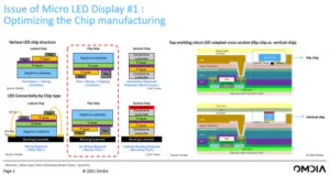
Anyway Kang started by looking at how to make the microLED chip itself. There are three basic concepts.
- ‘traditional’ lateral chips – these need to have wired connections, which makes fine pitch difficult
- Flip-chip – which has been adopted by ‘almost everyone’ with two pads on one side, so don’t need to be wired.
- Vertical chip – with pads at each end. In this case an additional ITO or other electrode layer is needed on top of the LED but the chip can be narrower. There is an additional burden for makers with the extra common cathode layer (diagram below).

Apple has a 2021 patent for its own design of microLED which includes its own driver circuitry under the LED which could make the mass transfer process more simple. X-Display has an alternate approach with the idea of putting the LEDs on a silicon backplane then transferring to the display.
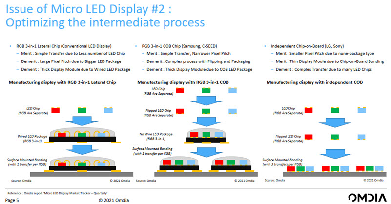
There is another challenge. After you have made the LEDs, how do you make a full colour display. Traditional LED display makers use packages containing three coloured lateral LEDs, but that adds another level of wiring pads and limits the pitch to larger dimensions. To get around this, Samsung and C-SEED among others are using 3-in-1 COB flip chips, but it makes the module thicker and means a relatively complex manufacturing process. Some, such as LG and Sony are using independent RGB flip chips without packaging in a COB configuration which allows a thin display module, but has the challenge of dealing with the mass transfer of more chips.
Another approach is to use QDs for colour conversion of blue LEDs (Saphlux/Nanosys) and the companies involved say this makes things simpler.
Another challenge is in the backplanes – whether the microLEDs are directly on a silicon wafer for AR/VR applications or are distributed over an area for larger displays. In the first case, the method of bonding the LED to the silicon is critical. In the second, makers are generally trying to make modules at smaller sizes (e.g. 10″/25cm) and combining them for a full display. In this case you have hide the wiring of each module. If the wiring is visible, it is distracting for the viewer. Panel makers call this ‘seamless’ technology.
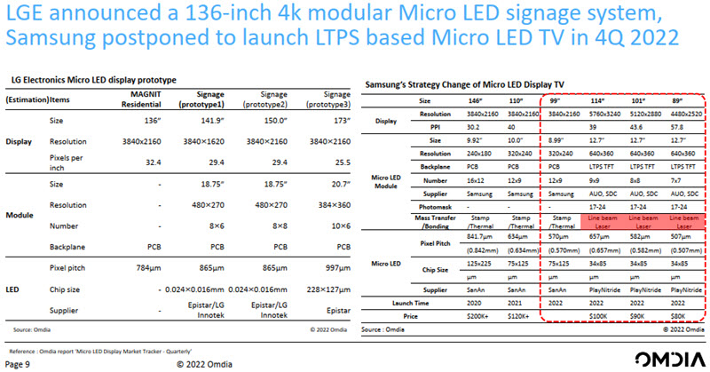
Currently the latter technology is not available on a glass substrate and PCBs are being used. Seamless technology is available for PCBs but LTPS glass-based techniques have been developed and Omdia expects to see them in the market by 2023. Samsung Electronics postponed its launch to Q4 this year, but this is likely to be postponed again because of issues with the LTPS backplane. LG Electronics is developing an UltraHD 136″ set based on LTPS and hopes to ship in 2023.
Turning to the well-known issue of mass transfer, Kang said that with 4″ wafers for LED manufacture, you need a way to get the LEDs onto the substrate for a TV-sized display from a number of wafers. Stamping has been used, but this is tricky so makers are trying to use laser technology. It is easier to adjust the pixel pitch, but laser equipment is expensive. For monolithic displays, you can cut up the wafer into complete displays.
Jade Bird Display (JBD) has started to make native colour microLEDs on silicon and Oppo, Vuzix, TCL and Xiaomi have made AR products using the displays. Kang then showed a useful slide that describes the features and pros & cons of different on-Silicon approaches to making small displays.
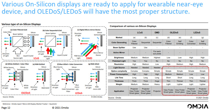
LED on silicon can be bright and doesn’t need the external light source of DMD and LCOS which makes those technologies bigger.
Moving to repair and defects, a lot of repair seems to be inevitable and ETRI in Korea has developed the SITRAM process.
Finally, as the LEDs get smaller, you have to change the bonding material (Bumping technology) from solder paste to copper to indum. Indium is best for the smallest chip.
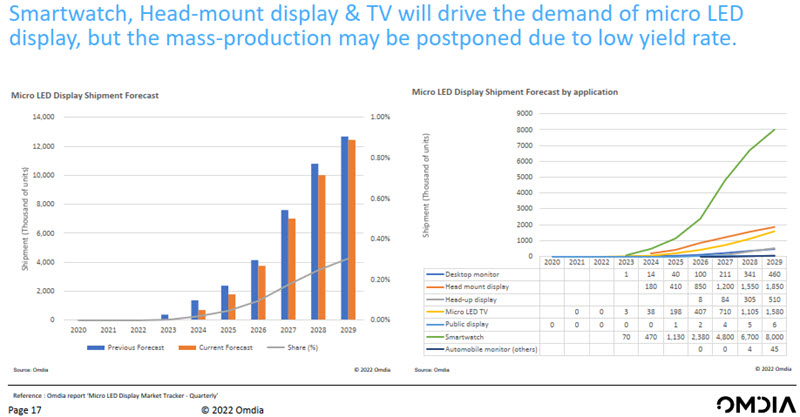
In summary, the microLED manufacture process is not yet standardised and progress in that is essential for market growth. Nevertheless, Kang presented Omdia’s forecast which sees smartwatches as the main volume application from 2023 onwards.
To meet the forecast, costs can and will drop over the next few years from $25k for an UltraHD 75″ in 2022 to just under $3,000 by 2028. That will allow a big increase in volume.
In questions, Kang said that he couldn’t currently say which is the best mass transfer process as there are many and also many different applications and LED devices. Many will compete and eventually winners will arise in the market. (BR)