I’ve been enjoying the recent TechBlick virtual event this week and I couldn’t resist a third article covering miniLED and microLED and hear from one of the key players, Epistar. (TechBlick did a great job in the range of speakers at the event).

 Dr SY Deng is from Epistar of Taiwan and his talk was titled ‘The Way from Mini to Micro LED Display’. Epistar is a specialist in LED chips and dies as well as solar cells. It has around 5,700 staff. From 2021 was integrated with Lextar (which packages LEDs and makes modules) and Unikorn which makes Advance Compound Semiconductor in a holding company, Ennostar.
Deng went through how Epistar had moved from a start in 1996 to have its chips in 50% of all mobile phone keypads by 2006, 40% of all notebook backights by 2008 and the same number of TV backlights by 2008 and by 2012 it was making 50% of all the LED chips in Taiwan. It became #1 globally for high brightness LEDs for automotive and sensing and after developing miniLED in 2018, its chips were in 90% of all miniLED tablets (which means, of course, the Apple iPad Pro – editor).
His talk focused on two areas, the critical issues for miniLED and then how the industry moves from miniLEDs to microLEDs.
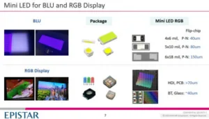
miniLED for BLUs and RGB Displays
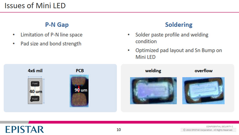
In backlights, there are a range of packaged and flip-chip configurations used. The critical dimension for different kinds of chips is the P-N gap. For example, a flip chip miniLED of 4×6 mil (0.1 x 0.15mm) would have a P-N gap of 40?m, but a larger 6×18 mil (0.15 x 0.45 mm) would need 150?m. At gap sizes of >70?m PCBs with High Density Interconnects (HDDI) can be used but down to the smaller sizes, glass or BT resin substrates are needed.

The Apple iPad Pro was a state of the art miniLED design in 2021 and has more than 10,000 miniLEDs (8×8 mil) and using Chip on Board (COB) technology to create more than 2,500 dimming zones with 1,000 cd/m² output (1,600 cd/m² peak).
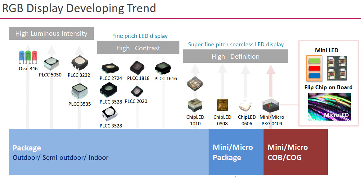
RGB LEDs are still developing to smaller pitches for outdoor use at pitches of 5mm or more. Epistar defines fine pitch as from <5mm to 2mm and pitches below as ‘super-fine’ for high definition. ChipLED forms in packages from 1010 (P1.6) to 0606 (P1.) and moving into miniLED at around P0.8 or below 1mm. For even smaller sizes, the architecture moves to COB or Chip on Glass (COG).
The major issue for miniLED is the P-N gap and the limitation of the P-N line space. As we have seen a 4x6mil miniLED has a P-N gap of just 40?m, but a conventional PCB needs around a 90?m gap between pads for reliability. It is also hard to limit the spread of the solder paste and there can be overflow of the solder/tin during the soldering process. A lot of work is needed to optimise the solder ‘bump’ and layout for miniLED.
Further issues include optimisation of the efficiency of the LEDs to avoid problems with the well known ‘efficiency droop’ which causes a drop off of efficiency as current increases. Another point to be solved is improving the quality of the chips and bonding to enhance yield when mounting the LEDs PCBs and on glass. Defect rates are also a critical issue in the longer term as direct view applications are brought to market with huge numbers of LEDs required.
Transitioning to microLED
Transitioning to microLED also has some challenges. As we have discussed this week, one class of microLEDs have the LEDs on a substrate and the whole substrate is bonded to a CMOS wafer for the control circuitry so that the device can be used in AR or VR.
For ‘sparse matrix’ (the term I prefer – editor) displays where the LEDs are spread over a bigger surface, a range of transfer options is available and being developed including laser, stamp transfer and self-alignment.
For backlights, you can use a single colour LED (blue) for the whole surface, but in microLED direct view displays, you have to disperse the RGB LEDs across the surface. The LED chips first have to be put onto some kind of carrier to be transferred from the wafer.
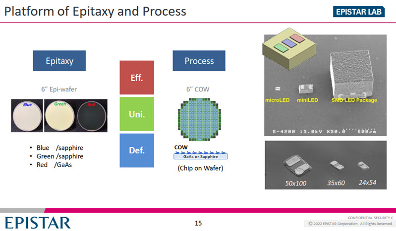
Turning to the epitaxy, blue and green LEDs are made on sapphire wafers, while red is made on gallium arsenide (GaAs) and efficiency, uniformity and defects are different on each. MicroLEDs are much smaller and thinner than miniLEDs which are much thinner than SND LEDs.
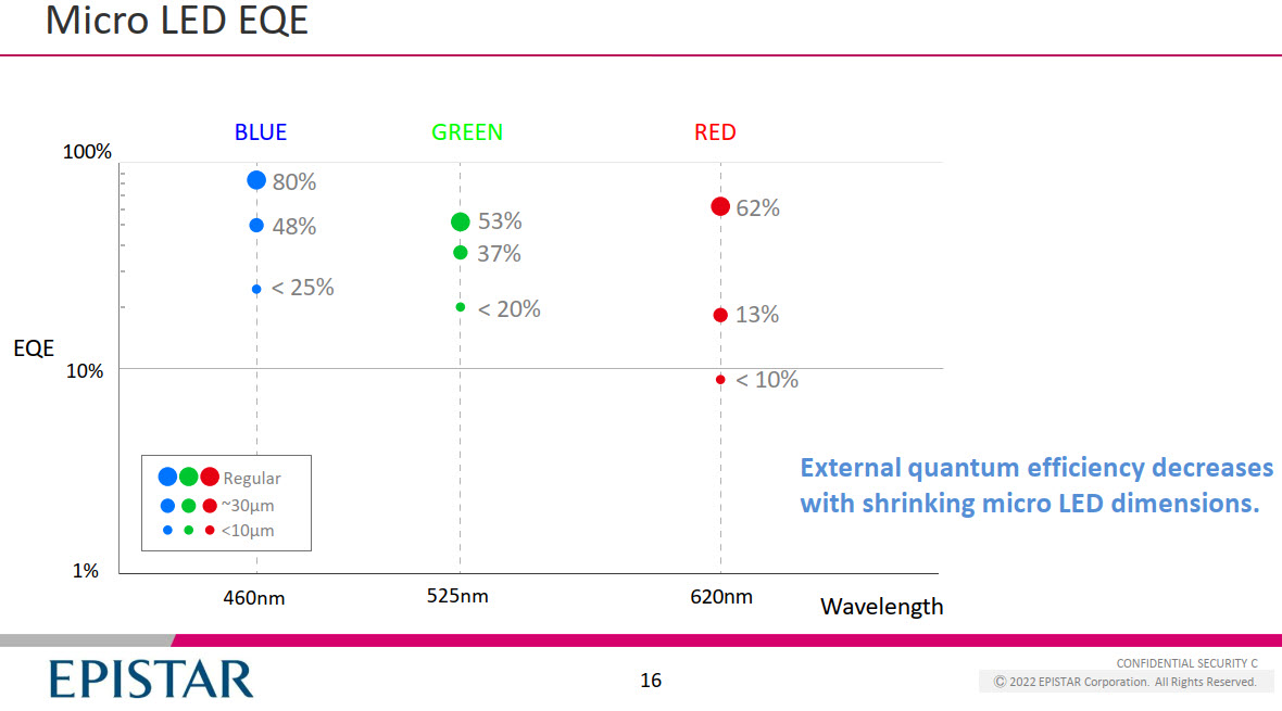
There is a well known issue of reducing efficiency with smaller LED size and this is particularly bad for red. Dr. Deng showed a nice chart that shows the problem for different die sizes.
Epistar can supply blue and green made on 6″ sapphire wafers and red based on 6″ GaAs. It can also make 8″ GaN on Silicon wafers for monolithic devices that need to be bonded to CMOS backplanes. (we have been reporting on the challenge that LEDs are made on 6″ wafers, but any advanced CMOS process uses at least 200mm wafers for a long time – editor). The LED dies can be supplied as ‘Chip on Tape’ (COT) or ‘Chip on Carrier’ (COG: glass, sapphire…)
Dr. Deng summarised his talk by highlighting for miniLED the number of devices used, the P-N gap issue, soldering and bond strength and efficiency. For microLED, the issues of efficiency, uniformity and defect density, the mass transfer techniques and the sheer quantity of dies needed.
I found this talk very interesting. It tied together a number of areas that I had been aware of but tied them together in a much more coherent way! Thanks, Dr. Deng! (BR)