Enter a new “breakthrough” transistor design from nVerpix for OLED pixels featured in this year’s iZone at the SID Display Week. With it, the group looks to resolve many of the key issues of OLED implementation and solves the problem, not with added transistors and the use of new materials (IGZO etc) but with a new pixel architecture that literally flips things around (OK, it pivots the architecture of the pixel.)
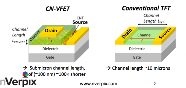
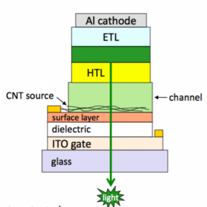
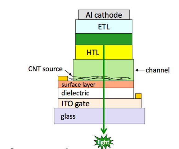
By re-orienting the transistor channel from horizontal to vertical, channel length is now defined by thickness of the thin film, giving sub-micron channel lengths that are approximately 100 times shorter than the conventional TFT approach, and done without high resolution patterning. This enables low cost (homogeneous) organics to be used in the channel.
In short, the mechanism consists of a dilute carbon nanotube (CNT) network (or graphene) that’s key to device operation. The group has created a Schottky barrier modulated device (the energy barrier for electrons formed at a metal–semiconductor junction), plus hole injection barrier from CNT to channel, modulated by gate, according to nVerpix CTO, Dr. Bo Liu.
 This approach adds the use of the third dimension to the OLED pixel problem. They are “…now able to use the whole area of the pixel for current flow,” according to Liu who took time to speak with us at the iZone booth.
Other benefits of the approach include an increased aperture ratio – from less than 30% to over 70%; lower current density through the OLED; a boost to materials lifetime; a much simpler pixel design (than even 2T+1C) circuit; plus a simplified manufacturing process that enhances yields.
The result is a full aperture light emitting transistor with no side-by-side drive TFT (that blocks pixel emitting area) using a CNT source electrode offering a whopping 98% transparency in a bottom emission approach, considered ideal for large displays.
Analyst Comment
So, as most will agree that OLED displays represent the long term future, with the promise of better brightness, viewing angle, response rate (reduced motion blur), lower power consumption, a thinner and lower weight design (using a smaller stack plus plastic substrate material) that enables flexibility, and even boosts shock tolerance. All this plus, in principle, a simplified manufacturing process, most also agree it’s still a tough journey until full adoption of OLED-based displays, especially of the larger kind.
Now many of the gating issues in moving forward with OLED displays are being addressed, not with new materials or increased transistors in the pixel, but a whole new pixel architecture (or rather transistor architecture that uses the 3rd. dimension of the pixel to deliver the goods (err… photons). Let the brave new world of OLED unfold, and thanks iZone for the heads up. – Steve Sechrist
(Ken Werner also highlighted this concept as being of particular interest)