
Ns Nanotech CEO, Dr. Seth Coe Sullivan presented at the northern California SID chapter on the status the company’s nanowire LEDs, which can be grown simultaneously in red, green and blue colors using indium gallium nitride (InGaN) on a single wafer.

The typical approach of using MOCVD equipment is limited to one color/wafer using InGaN for blue and green and AllnGaP for red, because growing red using GaN results in low efficacies that declines as the LED gets to the low µm level.
Currently, MicroLED displays come in three flavors:
- Very Large Monitors (TVs) – 80” to 500” that use relatively large LED chips (1mm²) compiled into modules and the assembled to the desired size
- Direct View Display – from TVs to smartphones that use 1-10 µm² die
- Micro Displays – for AR or MX that use 1-3 µm² die
Ns Nanotech has chosen to make µLEDs (nanoLEDs) for the AR market because they expect to produce red, green and blue LEDs on the same wafer. Today’s MicroLED micro displays are either monochrome, using blue die with a color converter or use three separate monochrome panels to create a full color display. NS Nanotech would grow all three colors using InGaN, side-by-side in the exact resolution of the target device. With no requirement to use color conversion or a color combination design, the Ns Nanotech solution use less power, be more efficient, thinner and cost less than other solutions.
MBE Rather Than MOCVD
Ns Nanotech uses molecular beam epitaxy (MBE) equipment to grow the LEDs rather than the more popular MOCVD tool. Monolayer deposition for super lattices and quantum wells is possible by both techniques with great precision. In MOCVD, reactant gases are fed into the system at high pressure ~ 1 torr whereas in MBE Ultra High Vacuum (UHV) conditions (i.e. pressures below 10-8 Torr) are required for deposition. The major differences between MOCVD and MBE are:
- MOCVD: Gases are let into the reactor at high pressure ~ 1 torr.
- MBE: Operates under ultra-high vacuum conditions, with pressures below 10-8 torr.
MBE is so precise that the film thickness can be controlled down to fractions of monolayers. MOCVD is less precise but still the thickness can be controlled down to fractions of nanometers. Thus, MBE is more precise in terms of the composition of the deposited films, which means a much bigger price of MBE vs. MOCVD deposition systems. Moreover, MBE equipment is generally found in labs, while MOCVD equipment is used throughout the world in mass production of LEDs.
The company had to invent new methods in order to overcome the current process limitations:
- Conventional InGaN quantum well (QW)-based LEDs suffer from wavelength/color instability, a result of the quantum-confined Stark effect (QCSE), which is manifested as a severe wavelength blue-shift with increasing optical excitation or electrical injection. Although nonpolar/semipolar III-nitride optoelectronics are being developed, achieving nonpolar/semipolar substrates with good quality and low cost remains elusive. The emission wavelength instability issue can be mitigated through coupling the emissions of µLEDs into a microcavity, such as a photonic crystal cavity or Fabry-Pérot cavity, wherein the dominant emission wavelength depends on the optical modes of the microcavity and is, therefore, less sensitive to the carrier density within the QWs. However, this method poses significant challenges in the device fabrication process and does not address the QCSE directly.
- The performance of green/red µLEDs remains limited since a relatively low growth temperature is generally required to achieve high indium composition, which significantly increases point defect density and impurity in the active region. When the lateral dimensions of InGaN QW µLEDs are shrunk to below the µm scale, the external quantum efficiency often drops to well below 1% due to surface damage-induced nonradiative recombinations caused by top-down etching processes. Moreover, there have been few studies of µLEDs monolithically directly grown on Si substrate due to the large lattice mismatch between GaN and Si.
Ns Nanotech overcomes these issues by adopting an AlGaN/GaN shell surrounding the active region with a negative Al composition gradient along the c-axis of InGaN nanowire µLEDs. The µLEDs are fabricated based on a N-polar nanowire array synthesized through a bottom-up selective area epitaxy (SAE) process. Detailed current-dependent electroluminescence (EL) measurements have shown negligible shifts in the peak energy. Elemental mapping and theoretical calculations show that the QCSE is largely eliminated due to polarization doping.
Strain distribution in InGaN QW is mapped using scanning transmission electron microscopy, which provides direct evidence that the use of AlGaN as the barrier can effectively reduce strain distribution in the active region and lead to enhanced indium incorporation. The devices have lateral dimensions below 1?µm and exhibit strong ultra-stable green emission. The µLEDs are grown on Si substrates instead of sapphire substrateS, which reduces thermal accumulation within the device area and enables seamless integration with CMOS electronics. The result is a viable approach for achieving high-performance µLEDs with highly stable operation on Si for ultrahigh-resolution full-color displays.
The nanowire µLED heterostructures are grown on a N-polar GaN/AlN buffer layer on Si wafer using plasma-assisted molecular beam epitaxy (PAMBE). As schematically shown in the next figure each nanowire consists of ~450?nm Si-doped GaN, six periods of InGaN/AlGaN multiple QWs (MQWs), and ~170?nm Mg-doped GaN.
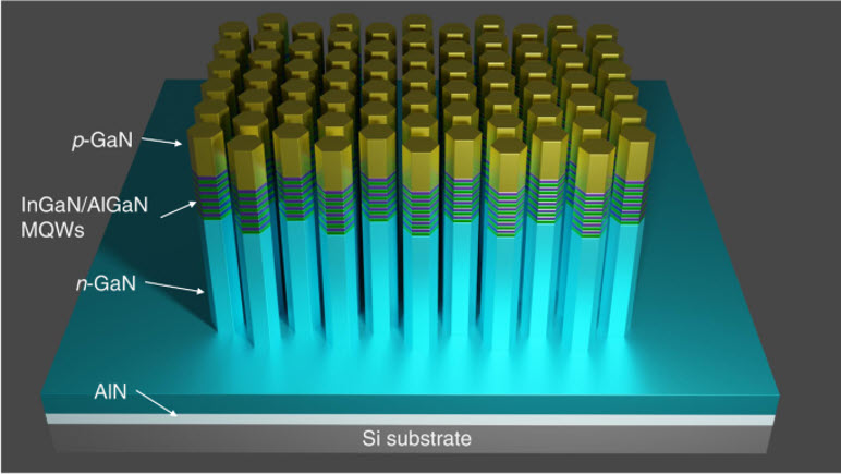 Figure 1: Nanowire µLED Heterostructures Source: Wu et al. Light: Science & Applications (2022)
The next figure is a SEM image of the nanowire array grown by SAE on Si substrate. Each nanowire is enclosed by six equivalent m-planes on the sidewalls and a flat top c-plane, contrasting the pyramidal (11¯0?11¯0n) top surfaces observed in metal-polar nanowires. The epitaxially grown nanowires inherit the lattice-polarity of the GaN/Si template, and the N-polarity is further confirmed by potassium hydroxide (KOH) etching.
Despite the high dislocation density within the GaN epilayer, the majority (>85%) of the nanowires feature nearly perfect crystallinity, indicating a filtering effect of the nanowire structure on propagating dislocations. The threading dislocation density (TDD) within the GaN film is measured to be ~3?×?1010?cm?2 41. The TDs terminate on the sidewall of the nanowires, as shown in the cross-sectional scanning transmission electron microscopy (STEM) image in the next figure (c), significantly reducing the defect density in the active region.
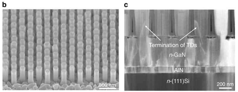 Figure 2: SEM Image of Nanowire Array and TDs Terminating in the Sidewall – Source: Wu et al. Light: Science & Applications (2022)
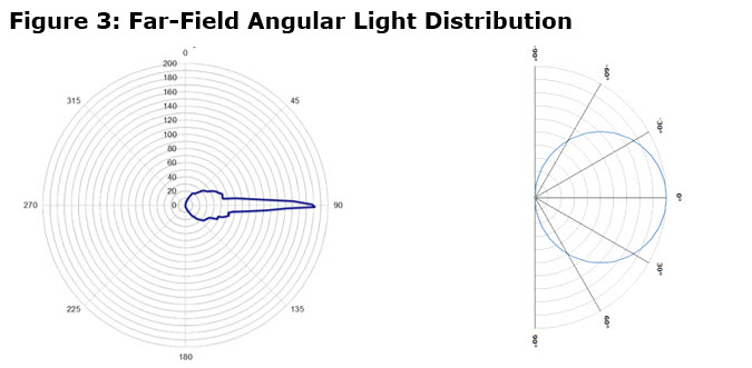
A periodic close-packed photonic structure is created where the photonic bandgap is independent of the electronic bandgap. This structure locks in the color regardless of the variance in temperature, doping or current. The emission cone is primarily normal to the device surface, which is an advantage in a micro display, but clearly has to be mitigated for direct view applications, which requires a Lambertian light source.
 Source: Coe Sullivan, Ns Nanotech
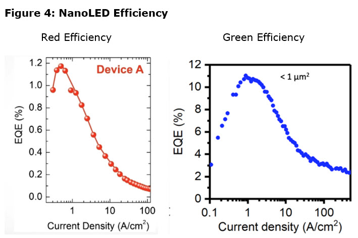
Ns Nanotech’s development is in an early stage and while the EQEs of the nanoLEDs, as shown in the next figure are relatively low compared to larger LEDs and OLEDs, the company claims performance records for 1µm red and green die.
 Source: Coe Sullivan, Ns Nanotech
Coe Sullivan believes that for AR applications, the emission cone, which is normal to the display makes better use of the available photons, when compared to a Lambertian distribution. However, typically AR devices use very thin lens to narrow the focus of the photons, but the very thin lens used today reduce the luminance by as much as 90%. Perhaps, the use of nanoLEDs could eliminate the lens or reduce the luminance loss?
Coe Sullivan did not provide a timeline nor was he able to estimate costs or reliability, but the AR market is still in its infancy and will take years to reach the level of performance that is needed to wear smartglasses all the time. However, potential competitors, MICLEDI and JBD have announced monolithic red InGaN µLEDs, while Porotech is designing color convertible InGaN µLEDs.
Ns Nanotech’s objective is to deliver a RGB Si wafer with multiple 1” (+/-) 8K configurations that can be sliced into display format and placed on a separately produced Si backplane to form a micro display with >100,000 cd/m² to meet the requirements for AR smart glasses. (BY)