A quiet revolution is taking place in the projected capacitive touchscreen market. Rapid industry developments are delivering touchscreens that are thinner, more reliable, lower cost and offer higher performance. The impetus behind many of these developments is the fact that ITO, the long standing conductive material of choice for phone and tablet touchscreens, has limitations and consequently is being superseded by alternative materials. ITO has never been widely used in large-format AV and kiosk applications, but some of the technologies that are being developed to replace it could.

Specifiers should be thoroughly aware of the underlying material being offered within their chosen touchscreen, as it could result in substantial differences in appearance and most importantly, performance in the field. Technologies that are very effective in one application may suffer from serious limitations in another. In this paper, we aim to help them make an informed choice, by reviewing six major alternative material technologies, and looking at the strengths and weaknesses of each. I will start by looking at why ITO is being superseded in some applications, and go on to examine the alternatives.
Why the move away from ITO?
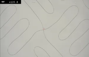
22” Zytronic multitouch 10um wire design
A key driver behind the changes in projected capacitive touch technology is the move to integrate touch into the LCD panel itself (‘in-cell’ technologies), eliminating the need for a separate touchscreen overlay (discrete touch overlay). Realising this results in thinner, lighter touch-enabled devices, which can be easier to integrate. Optical performance and brightness can also be improved by reducing the distance and layers between the LCD and the user.
However, the processes for manufacturing in-cell touchscreens are still evolving and improving and as a consequence, their widespread industry adoption has been limited. As a result, discrete projected touchscreens overlays using ITO conductors remain the principal technology, at least in smaller, handheld consumer electronic devices such as smartphones, tablets and wearables, but it suffers from drawbacks as the display size increases beyond around 20″, principally as a result of its relatively high electrical resistance, which hampers its performance and make it an unsuitable material choice for some applications.
So what conductive materials are available for larger sized touchscreens? There are presently three main material technologies at the forefront: Copper Micro Wires, Silver Metal Mesh and Silver Nanowires, with three more – Carbon Nanobuds, Conductive Polymers and Graphene – all in early stage development and likely to emerge in the coming years. We’ll look at four key parameters: economics, resistance, visibility and availability for the first five of these, and will conclude with a look at graphene, which really is in early stage development and isn’t commercially available at the moment.
Economics
Some of the key issues when considering the cost of touchscreens are initial tooling costs and ongoing material requirements. Technologies that can be directly written to the substrate materials without a mask require little in the way of tooling and can be produced more cheaply in low volume. If masks or other tooling is required, then this limits the ability to produce screens of different sizes flexibly in low volume, but has the potential to offer reductions in high volumes on standard sizes.
In terms of tooling, copper micro wires score in terms of flexibility. The electrode can be written directly to the substrate, with no lasers, masks/chemicals/etching or tooling needed. Silver nanowires can be customised to a degree, via laser ablation, but then additional processing is required to link the conductors at the borders to the controller. Conductive polymers are also applied relatively easily with screen printing; however, they need to be patterned at either the silkscreen printing stage or after with etching or lasers.
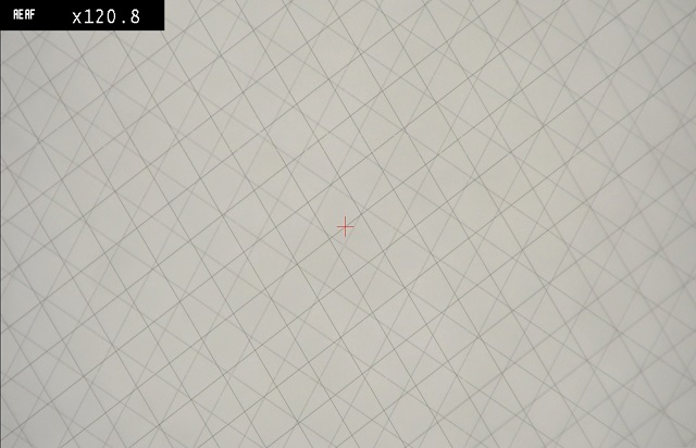 22″ metal mesh 4um designBy contrast, silver metal mesh materials are patterned at source, so the size of sensor needs to be specified upfront. This leads to tooling charges which can range from around $10,000 to $20,000 per sensor design depending on screen size. The procedure to deposit the carbon nanobuds is complex, using a ‘nanobud reactor’ then a laser patterning process to create electrodes.
Another key factor in manufacturing cost is the number of layers required. Copper micro wires can be insulated, so that the x and y electrodes can be formed in a single layer. The encapsulating insulation also prevents oxidation of the material, which can seriously degrade touchscreen performance when exposed to high heat and humidity in the field. Silver nanowires, metal mesh and conductive polymer sensor constructions generally require two or more layers to insulate the (x and y) conductors, increasing the material content over a single layer design. Carbon nanobuds are also a two-layer technology. Furthermore, care must be taken to prevent moisture ingress into the materials, which can cause the above noted oxidation and touchscreen failure.
Resistance
Touchscreen resistance is a key factor in determining sensitivity to touch, or ‘signal to noise’ ratio (SNR). Higher resistance materials limit the amount of current flowing through the conductors, making it harder to correctly pick out a touch event from surrounding ambient interference (EMI) coming from the display, power source or other surrounding electronics. Clearly, this resistance becomes more of an issue with larger touch screens, especially if features like multi-touch, palm rejection and proximity detection (identifying a touch before the finger actually makes contact with the screen) are required.
As indicated above, ITO has generally been limited to smaller touchscreens due to its relatively high resistivity of ~100 ? per square. As a result most touchscreens using this material are smaller than about 22”, beyond which there are significant performance limitations. Silver nanowires have a better resistance than ITO (~30 ? to ~50 ? per square on PET film substrate). As a result, projected capacitive touch sensors using this technology are scalable up to around 42” (beyond which, again, touch performance is hampered). Silver metal mesh has a lower resistance of around ~15 ? to ~30 ? per square, and as a result is capable of use in touchscreens up to around 65” in size. Copper micro wires offer the lowest resistance at ~5 ? per square or less, and can be used to create enormous touchscreens, well over 100” in size. Furthermore, the extremely low resistance provides the best signal to noise ratio, resulting in touchscreens that are capable of detecting touch through very thick overlaying glass and even gloves, without the need to drive the control electronics at high voltages or tile the screens using multiple linked controllers (both tricky methods used by alternative material technologies to achieve large size touchscreens).
Visibility
All discrete overlay projected capacitive touch technologies involve introducing some material element between the user and the screen, which will make some optical difference, however small, to the image. With copper micro wire-based technologies the grid of 10um conductors can be visible, particularly when the display is off. That said, light transmission is excellent and in the range of 90% before any anti-reflective treatments are applied. In contrast, silver nanowire and metal mesh technologies enable the creation of slightly less visible conductive tracks (metal mesh in the 5-10um range); however, nanowires and conductive polymer coatings can produce a slight colour cast or haze over the whole screen, and a base light transmission of around 85%.
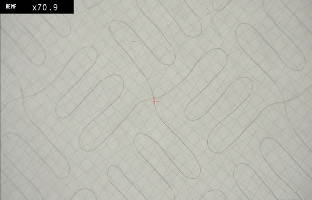 22″ metal mesh and multitouch designs overlaid for comparisonAvailability and longevity
Copper micro wire touch sensors have been in production for nearly 20 years by a handful of specialist manufacturers and are a proven projected capacitive touchscreen technology for large sizes in the harshest environments. Silver metal mesh and nanowire-based touch technologies have emerged into the mainstream quickly over the last few years, with many manufacturers installing the necessary printing and laser patterning equipment. The relative newness of these two technologies in the touchscreen world mean that their long term reliability is not yet proven – particularly in relation to how their resistance (and touch performance) changes as exposed to temperature and humidity in challenging, often outdoor applications.
Graphene
On the horizon is a potentially game changing new touchscreen material technology in the form of graphene. First discovered at Manchester University in 2004, there have since been promising results released on its strength, transparency and conductivity, but development is still in its relative infancy. Deposited as a one atom thick layer of carbon, it combines a similar low resistance to copper micro wire with the potential of ‘invisible’ conductors. However, despite its potential suitability as a material for projected capacitive touchscreens, there are many other applications for this exciting new technology, such as water purification, batteries and solar cells, and most developers are focusing their efforts on these areas for the present with touchscreen usage being much lower on the development roadmap.
The bigger picture
In conclusion, there remains no such thing as the ‘perfect’ conductive material for projected capacitive touchscreens – and designers should always look for the best combination of performance, optics, durability, scalability and reliability to suit their touchscreen application. The worldwide market for phone and tablet touchscreens dwarfs the commercial AV market – just to give an indication, Touch Display Research Inc. estimates that the ITO replacement market could reach $13 billion by 2023. As a consequence, new touchscreen material developments are inevitably focused on this massive market. However, the investment will almost certainly bring benefits to the commercial and industrial market too.
– Andrew Morrison
Andrew Morrison is the technical director at Zytronic. He initially worked in the display industry with LG Phillips Displays in Europe and the UK, before joining Zytronic in 2002. With over thirteen years of electronics, software and touchscreen development experience he leads Zytronic’s growing R&D team in which he is actively involved in all aspects of electronic controller and sensor development for their patented projected capacitive touchscreen technology.