Display industry is continuing its journey in the path of innovation for next generation products. Quantum Dots have become a technology platform from LCDs to OLEDs and MicroLED displays to printable electroluminescent displays. NanoLED is the new name for QDEL (electroluminescent) display.

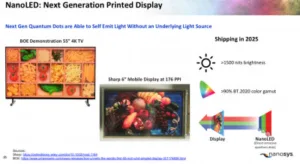
According to Nanosys’s presentation at DisplayWeek 2021 Business Conference, QDOLED display is expected in 2021/22, QD MicroLED in 2023/24 and NanoLED in 2025/26. NanoLED, an emissive display, has the advantages of perfect black, better color, and wider viewing angle. It also provides true HDR luminance and higher reliability (inorganic materials). However the biggest attraction for this next generation display is the potential for ultra-thin flexible displays at low cost with its solution process printed manufacturing.
NanoLED: The Name Change
QLED was an early name of QD emissive technology. It is also called QDEL. However the name QLED has beed adopted for QDEF-based LED TVs. Nanosys has now re-named the QD emissive display technology as NanoLED. According to Jason Hartlove, CEO of Nanosys,
”we opted for the name NanoLED as all the materials in the stacks are “Nano” materials and it is a Light Emitting Device (LED)”.
NanoLED is the future emitter material for QD emissive displays. The new name seems to be getting traction. The purpose of this nomenclature is to enable the industry for technology development.
Display Advantages
Nanosys presented a paper on “Heavy-Metal-Free Electroluminescent Devices” at Display Week 2021 (by Diego Barrera and team). The paper pointed out that QD emissive displays have the advantage of spectrum engineering. Precisely producing the desired spectrum also leads to higher power efficiency (no waste). Quantum Dots also emit light with narrow spectral peaks. By just tuning synthesis conditions at manufacturing a wide range of colors can be created.
QD emissive displays are very bright: about 614,000 d/m² (sunrise is 600K nits) whereas OLED can reach only up to 10,000 nits. Being solution processable, QDs are very versatile. They have been formulated with solvents, monomers, polymer films, inks, photoresists; and are attached to biomolecules, cells and more. The paper specified that quantum dots are lower cost per gram than current phosphors. As QDEL are solution processable they can be transfer printed, solution printed or gravure printed in future.
The Blue Gap
Due to RoHS and other requirements on the industry, QD emissive display requires Cd-free (Cadmium free) QDs. Heavy metal free QDs are catching up to CdSe (Cadmium Selenide) QD in performance. They have been able to create InP (Indium Phosphide) QDs having a similar level of QY (Quantum Yield) performance as CdSe dots.
Nanosys’s “Heavy-Metal-Free Electroluminescent Devices..” presentation at DisplayWeek showed that controlled synthesis of QDs with cubic morphology has also resulted in significant improvement of heavy metal free QDELs. They have been able to achieve highly efficient InP QDs with narrow spectra for red and green. Red and Green lifetime and performances are very good.
However, they have a ‘blue gap’. The blue target wavelength is 450-460nm and the InP QDs are efficient for >500 nm and ZnSe (Zinc Selenide) QDs are efficient at <440 nm. There is a gap between 440-460nm for efficient RoHS-compliant QDs. By modeling Nanosys has found ZnTeSe alloy QDs to fill the blue gap. They were able to get ‘true blue; at 452nm. They have made great progress on true blue Cd-free material.
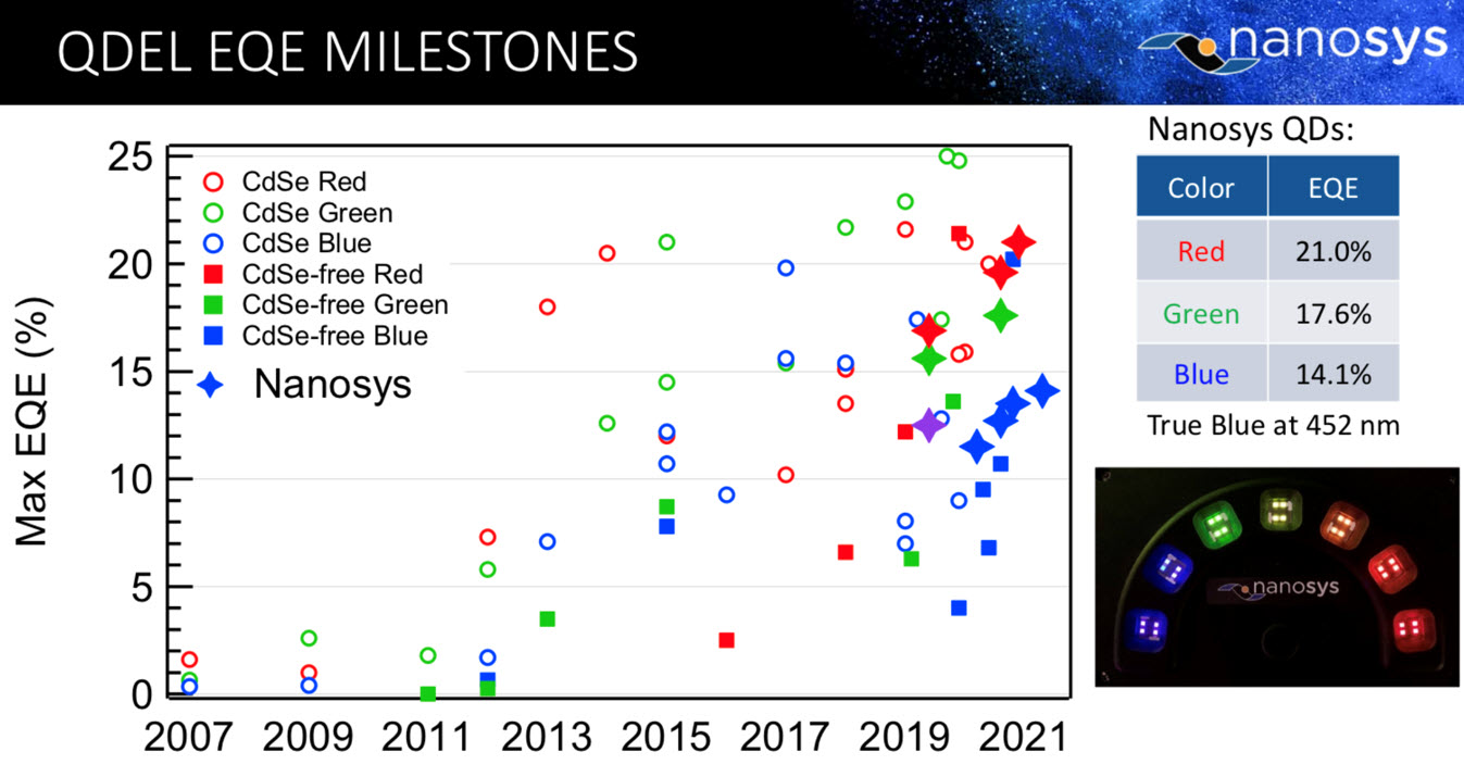
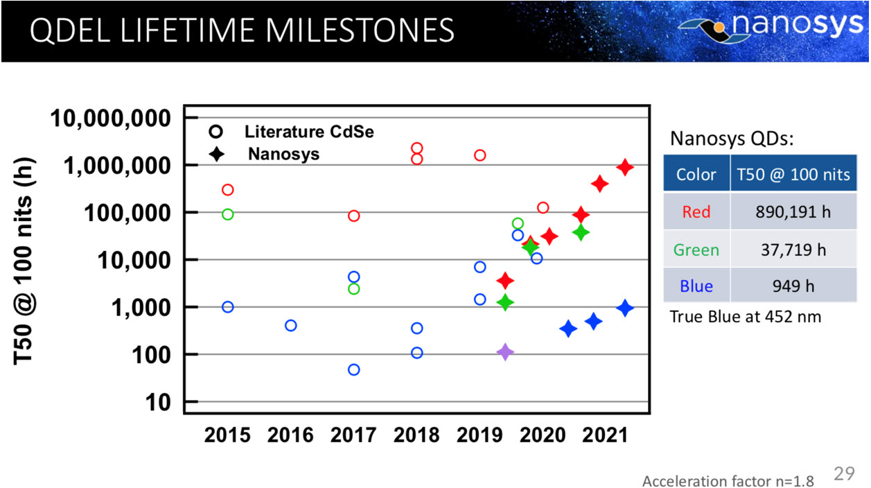
The firm has demonstrated high EQE (External Quantum Efficiency) for all colors: R/G/B = 21.0/17.6/14.1%. QD emissive lifetime for true blue is still lagging, though. While red’s lifetime is closer to 1,000,000 hours, green 40,000 hours, but blue is less than 1,000 hours. Researchers need more time to perfect their ability to customize the crystal to get emission character and lifetime. These are material challenges they need to overcome. According to Jason Hartlove,
“for blue material challenge, we will have linear rate of progress towards lifetime. It doesn’t depend on a breakthrough”.
They believe they can propose a timeline for the solution. They have started working on these new materials from 2019. According to Nanosys data they have made more than two orders of magnitude on lifetime improvements and 24% efficiency gain during the 2019 to 2021 timeframe. Time is needed just for blue. Red is ready for commercialization but not for RGB applications.
Scalable Manufacturing
The NanoLED manufacturing process is said to be very scalable with potential for lower cost. With a solution printed process you can break the paradigm of needing large substrates and multi-billion dollar investments like LCD or OLED. The economic argument is compelling.
According to Jason Hartlove,
“cost will be one tenth (1/10) of the equipment cost for factory for solution process vs. vacuum deposition. With solution printed process you break the paradigm that you need gigantic substrate, also yield management, size of tools, and size of the factory, all change dramatically”.
There is no need for minimum increment for fab size or production like high Capex manufacturing of LCD or OLED, to make it profitable. For solution-printed manufacturing, you can have a smaller factory with small footprint that can still produce larger size displays.
According to Nanosys, a $200 million factory can make large size products in small volume and with the potential for profit. This can open up opportunities to make products closer to the consumption location, resulting in an improved supply chain. Suppliers who couldn’t invest billions of dollars for 10.5 Gen LCD fabs or 8.5 Gen OLED fabs could manufacture this technology. They have to establish an appropriate supply chain. Solution process will develop much faster. Inkjet printing is already here but other printing technology can come in the future to make it faster.
Lower costs
This makes NanoLED emissive displays fundamentally disruptive. Unlike OLEDs or LCDs, QDEL devices can be made using only solution processing. This means devices can be significantly lower cost to manufacture, opening up many new applications for displays where today only printed materials are used. This kind of ultra-low cost printed display technology is making rapid progress towards commercialization.
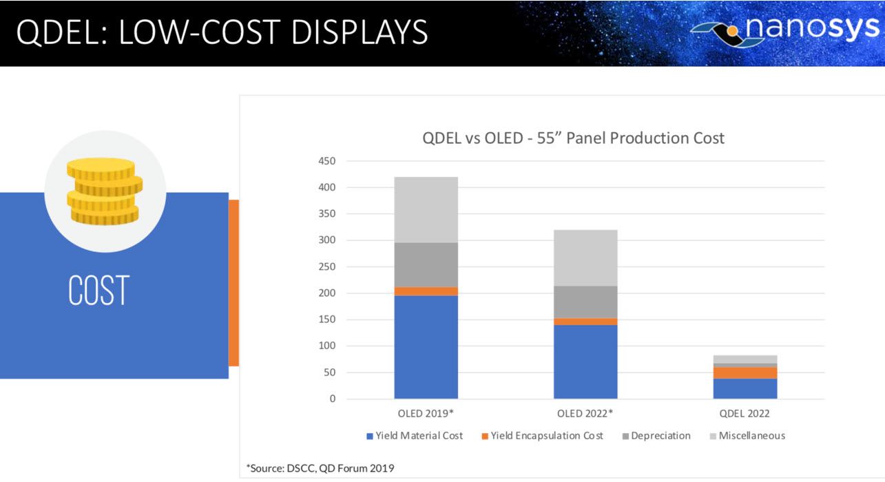
Suppliers can still use their existing glass based backplane technology with LTPS, IGZO, LTPO or others. Glass is not a requirement. Makers can use other flexible backplanes; where they can print on flexible substrate directly with design dependent on panel width or panel length. Production can be based on continuous feed or semi-continuous feed ‘sheet by sheet’. While backplane technology can stay the same, the frontplane technology will be solution printed. This process is new for display. Nanosys has made demoes in the lab and their partners have created prototypes and the technology can be scaled to mass production. A model cost calculation from DSCC showed that a 55-inch QDEL panel cost can be substantially lower than OLED.
Supply Chain Disruption
QD emissive display has the potential to disrupt traditional supply chain, as all the materials can be changed the players can also change. NanoLED display manufacturing will have substrate vendors, tool vendors, and material suppliers, display panel suppliers, and component suppliers, as well as open cell opportunities. Traditional suppliers can continue to innovate and be part of the new supply chain.
In an emissive QD display there can be 3 to 5 thin layers of QDs and needs semiconductor levels of purity. All stacks need to be encapsulated and thin film encapsulation (TFE) will be very important. While the encapsulation requirements for Quantum Dots have been lessening and materials are getting more robust, for the most part the narrow spectral emitting, non-heavy metal materials still require packaging and processing. This adds cost to a solution using quantum dots.
Over the next few years, advances in making quantum dots more environmentally stable, as well as progress in the availability of low cost encapsulation materials and technologies will help the industry. The supply chain for the display industry has been evolving with each new technology. It evolved when the industry shifted from LCD to OLED and it can also evolve again to get ready for NanoLED.
Traditional and New Application Market
Being able to print NanoLED to other substrate creates new paradigm opening up new substrate and new applications. Higher brightness, lower costs and new form factors can be big advantages for NanoLED. According to Hartlove,
“for future of NanoLED for direct view applications, we are focusing on, much lower cost, new substrate, new manufacturing techniques, that enables displays to be made and put on surfaces that so far we have not seen. Last time we had that breakthrough was flat panel technology.”
Looking at NanoLED display performance in terms of resolutions and brightness combined with its flexible conformable form factor and lower cost manufacturing capabilities, suppliers feel NanoLED can have an opportunity in all direct view display applications (smart phones, tablets, computers, TVs, Signage, retails and others) in future.
New application such as tables in the restaurants in wood or metal surface can be used for completely solution-based displays. NanoLED is inherently flexible. As a self-emissive display, it can also be transparent and has the potential to revolutionize the display market. For example it can be used in autonomous vehicles on the window shield. It can also be used in retail environments to enhance the shopping experience.
MicroLED with its much higher brightness (>1 million nits) and very high resolutions can be very successful for indirect display such as AR, HUDs and others. According to Russell Kempt, Nanosys’s Marketing VP,
“OLED has proven to be very valuable for many applications, however for very bright and very high PPI displays there is need for Micro and NanoLED.”
OLED is generally <10K nits brightness (although Kopin has said it has achieved 35,000 Nits). MicroLED and NanoLED can provide that.
To quote Hartlove,
“MicroLED is a superior technology for indirect display. Both Micro and Nano technology will bring new form factors to application developers and product developers. That is very exciting”.
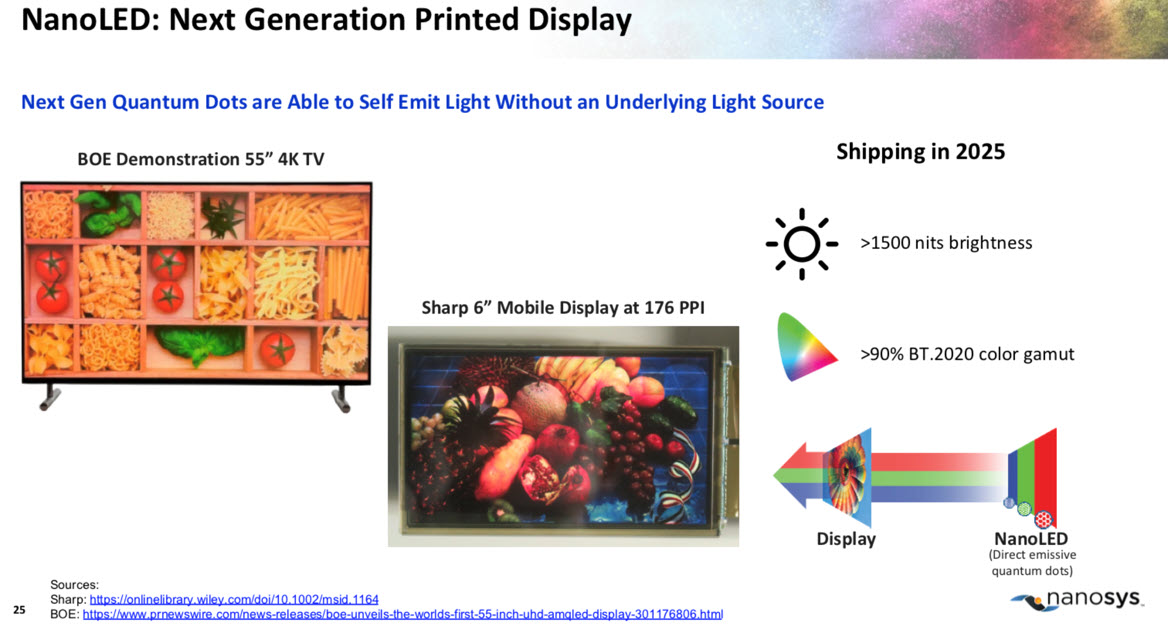
Many suppliers are currently working on QD emissive display products. BOE, a partner of Nanosys has shown a prototype 55″ TV at DisplayWeek 2021. Sharp has also shown a 6″ mobile size QD emissive display with close to 200 PPI and full video capabilities.
Conclusion:
NanoLED with Cd-free, heavy metal free quantum dots has great potential to become a next generation display technology because of:
- simple device structure,
- higher performance,
- higher brightness,
- flexibility, and
- low cost printing patterning scalable process.
Developments need to continue in terms of materials, printing, encapsulation processes, equipment and the supply chain to bring products to market. The success of NanoLED will depend on suppliers’ ability to produce higher performance and lower cost products to meet next generation product requirements. (SD)
Sweta Dash, President, Dash-Insights
Sweta Dash is the founding president of Dash-Insights, a market research and consulting company specializing in the display industry. For more information, contact [email protected] or visit www.dash-insights.com