Our front page story from Sony was not difficult to choose this week. We have a special “microsite” with news from SID’s Display Week, which starts in a couple of days. In my introductory article for this page, I said “Micro LEDs – there will be much discussion of whether this can be a disruptive technology (“The Only Disruptive Technology at Display Week”)”. On Wednesday, I spoke to an executive from a company that we consult for about future display trends and briefly explained that I saw microLED as a genuine potential game changer. I hadn’t expected to see the kind of announcement from Sony that we feature on the front page the next day and, frankly, I would have expected to hear something at SID, rather than Infocomm, as SID tends to look further into the future.
I had the chance to see the CrystalLED demonstrator from Sony at CES back in 2012. It was a very impressive demonstration, but there was no suggestion of an early commercial product. However, the Infocomm announcement from Sony of its CLEDIS technology looks much closer to a finished product, with an expected shipment date in early 2017. The pitch of the LED system that Sony announced is about 1.2mm (not that extreme – others have already got to 0.7mm pitch LED in production). The 1.2mm pitch means that the resolution is about the same as a 105″ FullHD display. Sony says that the actual pixels are very small, so, presumably they could be mounted closer together? Would that open up the possibility of higher resolutions? It would seem so, which might open up the technology to the possibility of moving into the TV or even monitor and portable device worlds.
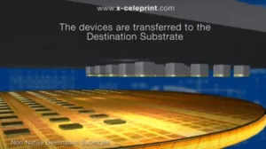
That would depend on price, which is a combination of the cost of the LEDs themselves and of the driver systems. Sony has not released any details of the types of LEDs that it is using – we’ll try to find out more when we get to Infocomm. However, companies such as X-Celeprint are doing work on systems that use a system of growing LEDs on the surface of a wafer using epitaxial growth, which can then be transferred using printing onto a display surface. (See Back to the Future… by Candice Brown-Elliot). This concept appears to mean a significantly lower cost for the LEDs than directly using wafers (I have written in the past about the cost challenges if you simply try to chop up wafers: LEDs – How Far Can They Go?).

Now, if you want to get the cost down, you also have to build in the control of the pixel into the substrate, rather than using separate controllers as Sony is doing in its new system. That means probably putting tiny segments of crystal silicon close to each pixel, but should be achievable using the same manufacturing techniques used for positioning the LEDs, as Candice pointed out. As long ago as 1999, Alien Technologies, a US start-up, had ideas of doing this, although that company pivoted to create RFID components rather than displays.
So, we have some way to go with microLED, still, but the Sony announcement has ensured that it will be a hot topic for the next three weeks, when I will be at SID, AWE and Infocomm and I look forward to meeting many of our subscribers and friends at the San Francisco, Santa Clara and Las Vegas events!
Bob

