
Many years ago I saw a LED Wall with a pixel pitch of 1mm and was intrigued by the opportunities that such a technology could bring to a low power cinema or TV display solution for the home. Still, to this day, the promise of the LED wall as a low power alternative display technology for entertainment purposes is mostly unfulfilled. Every year at InfoComm and other professional display shows we see LED walls as a solution for high brightness digital signage that is meanwhile good enough to show video.

Depending on the manufacturer, you still do see brightness variations of the LED tiles. Some are showing sub-millimeter solutions that are often marked as development units and sold at significant price premium over the typical 2-8mm LED walls that rule the world today. Now we hear about these startup companies that are working on micro LED displays to enter the world of large size as well as mobile display panels and want to compete with LCD and OLED panels.
The term microLED goes back to research by LED makers and universities who were looking at using a chip level approach to creating LED backlights. Of course, it is easy to see why one would work in that area if one wants to sell more LED chips. Once LED chips became cheap enough this was considered a potentially viable solution. There are many flavors of microLED displays in the works, including direct view RGB LEDs, quantum dots on blue emitters, white LED with color filters, etc. If you can think of it, somebody has been exploring it.
Meanwhile some of these start-up companies have been bought by larger CE companies like Apple and more recently by Facebook/Oculus as potential solutions for mobile devices. This is where it gets interesting as these companies are targeting quite different panel requirements. But we will discuss this a little later.
 Source: TechNews.com
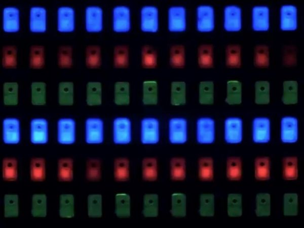
At a first glance, these microLED companies are the continuation of the developments of the LED wall makers. However, this is only true at first glance and for some of them. The LED wall makers are using packaged LEDs that are combined on a PCB as closely as the LED packaging allows.
MicroLED companies, likeSony and InifiniLED (now Oculus) are using pick and place approaches to get the discrete unpackaged microLED chips onto a substrate. In this case we are talking about micrometer scale parts being assembled compared to the millimetre parts that are being used in LED walls today. LED walls are created by soldering LED packages to a PCB, a process that will need complete rethinking when applied to parts that are smaller by three orders of magnitude.
As a matter of fact, most of the IP generated by these microLED startups revolves around placing and connecting LED semiconductor chips on an active matrix TFT backplane. To make this even a little more complicated, in most cases this includes some three dimensional structure to decrease photon losses within the structure.
Source: Sony Cledis
In the case of Sony, the empty space around the LED pixel is very large, while for some other displays the ratio of LED chip versus empty space approaches almost 1:1. This is of course a direct consequence of the resulting pixel density, which is determined by the resolution and the panel size. For applications where pixel densities of 1,000 ppi or higher are desired the solution maybe more of a wafer manufacturing process with a lift-off process similar to what Kopin is using. It is almost ironical that Kopin’s background goes back to III/V (LED) devices, a business segment they sold some time ago.
While some are very keen to use the black space around the LED chip to enhance contrast for large size displays, the others want to create a LED wall on microscopic scale that allows for very low power consumption and high brightness. Indeed, the latter requirement is where today’s LCDs are hitting the limit of their technology. While OLEDs are already replacing LCDs in mobile applications, the even better efficiency of semiconductor based LEDs may lead to a rather short time leadership for OLEDs in the very small display space. A similar situation exists for the virtual headset space, where higher pixel densities will lead to better imagery for VR.
One of the expected application targets is the Apple Watch, where peak brightness and long battery life will rule in the long term. Who wants to charge their watch twice a day if you use it a lot outdoors?
Of course the microLED display also offers better power efficiency for TVs, which many believe is of no consequence, as TVs are typically connected to a wall outlet. I just want to remind everyone of the ultimate fate of the PDP displays when power savings regulation more or less pushed PDPs out of the market. This will of course not happen over night, but if microLED based systems can save substantial energy over a LCD/LED or OLED display, political pressure will mount. In a country like the US, one step in the Energy Star TV regulations eliminates the need for a new power plant.
The remaining question is of course if and when such microLED displays can be manufactured cost effectively. Well, this sounds just like another engineering problem. Right? – Norbert Hildebrand