Hardly a day goes by without another market research company anticipating that microLEDs will dominate the display industry or that another start-up has made a breakthrough to enable cost effective product development. Yet the only commercial µLED products released to date are very large, very expensive TV monitors from Samsung, Sony and LG.

Sony released the first product called “Cledis” back in 2016 and no new applications have since been announced. The technology has been handicapped by the underperformance of red and green LEDs and the lack of a fast, low cost method of transporting LEDs from a wafer to a display substrate.
Recently, A French start-up marginally associated with CEA-LETI has been raising $140m to add to its capital of $80m to pursue both RGB LED production on a single silicon wafer and a unique, low cost, high throughput approach to transporting the µLEDs from the wafer to the display substrate. (Aledia Gets Investment for Manufacturing)
We take a dive into the economics of Aledia’s approach relying on the general comments of their CEO and the performance of Jade’s 0.3” monochrome µLEDs that deliver 1 million cd/m2 as a starting point. The results are surprising as we compare Aledia’s RGB solution to the use of blue µLEDs with color conversion vs. RGBW OLED, IJP OLEDs and LCDs for TV panels and RGB (side-by-side) for smartphones. (The cost comparison will be in part two, tomorrow – editor)
LEDs, whether standard size >100µm, mini 25-100µm or micro 1µm to 25µm, are grown in monochrome structures, either all red, green or blue. Since blue LEDs have 25% higher EQE than red and 50% higher EQE than green, most energy dependent applications, e.g. lighting, backlights and µLED micro displays use blue with some form of color conversion. Down conversion results in a loss of light output, for example, color filters reduce luminance by ~67%, quantum dots have 90% absorption and both approaches add costs. The LED industry expects the efficiency of red and green to eventually reach blue performance. But even in the most optimistic forecast, the difference won’t be resolved until 2040 or 2050.
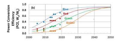 Figure 1: Efficiency Improvements of LEDs Over Time. Source:DOE
Micro LEDs have even lower efficiencies as EQE varies with size as shown in the next figure published in Nature.
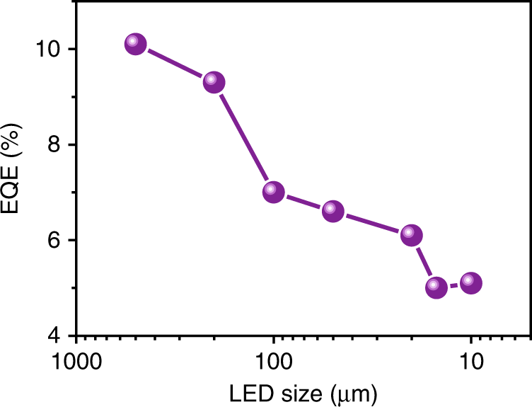 Figure 2: LEDs—EQE vs. Size.
Source: Nature (“Micro LEDs” w/QD in Display Technology)
Given the opportunity to disrupt the $100b+ display industry, microLED manufacturers are seeking every opportunity to reduce the costs of transferring µLED from a sapphire or silicon carbonate substrate to a glass or plastic substrate for use in a display.
Jade Bird Display recently announced a state of the art, 0.3” monochrome Micro LED panel on glass with red, green or blue monochrome uLEDs. To increase the efficiency of red and green to blue µLEDs, researchers are looking to reducing the size of the emitters to nano levels and using Ga N for all red as well as blue and green.
We described such an effort by NS nanotech, previously in Display Daily (NS Nanotech Solves the Binning & Green Gap Problems for Micro LEDs and A New Means to Produce Transparent Conductors Based on Nanotechnology) . Display Daily also featured a report on Aledia, which according to the author is accelerating µLED execution.
Aledia is a French start-up, in the process of raising $140m of which, $80m is committed according to President, CEO and cofounder, Giorgio Anania to accelerate the development of its nanowire on silicon microLED technology. Previous investments included a Series B and C rounds for a total of $77m.
Most LED makers grow GaN on a sapphire substrate, (although SiC is also used) as it exhibits good efficiency and is long lasting but has size limitations because of its crystalline nature. Red is based on AlInGaP , which is highly temperature dependent – small changes in temperature lead to large changes in color, efficiency and reliability, so relatively low operating temperatures are used. InGaN has lower dependences and can operate at higher operating temperature. In an RGB configuration with two different materials sets trying to co-exist, the system must operate at the “wrong” temperature for one of the materials or somehow create two thermal planes to support each material. In addition green has proven to have low efficiency when grown using GaN and exhibits the well-known “green gap”.
Aledia intends to grow single crystalline GaN nanowires (NWs) on a Si substrate with uniform growth orientation, which helps the nanowires produce highly efficient optoelectronic devices. A similar approach can be used to grow other compound semiconductor nanowires. They expect to extend the upper size limit of the GaN growth area to produce red, green and blue light from GaN nanowire-based bright LEDs grown on fused silica based on enhancing the electron current channel, which is the wetting layer. By keeping the base structure at the nano level, GaN can produce any color without sacrificing LED performance.
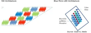
Aledia is using MOCVD equipment from Veeco and has a target date of 2023 for mass production. Nanowires enable the production of nm LED emitters and multiple emitters are used to produce a sub-pixel of ~1um, The next chart is a cartoon representation of the differences, between the use of NW µLEDs and using blue µLEDs with color converters.
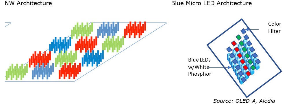 Figure 3:RGB Vs. Blue w/Color Filter Architecture
2D Micro LEDs use blue LEDs with a phosphor to convert the light to white and then a color filter to create red, green and blue sub-pixels. Alternative QD color converters could be used to convert blue to red and green, but a color filter might still be needed.
Nanowire RGB designs offer several benefits over the 2D approach:
- No conversion from blue to white
- No color filter that blocks 80% of the light
- Built in redundancy, since multiple nanowires are used for each sub-pixel.
Aledia wants to use NW RGB LEDs to compete with OLED based displays for TVs and smartphones and virtually every other type of display application now using LCDs. Aside from the growth of NW LED emitters, Aledia is working on a novel transport mechanism that will transport the NW µLEDs from the Si substrate to a glass or plastic substrate to make direct view displays. While Aledia provides very little technical info about its NW technology, they have provided absolutely nothing about the transport technology.
The key elements of the NW technology include:
- Using Si instead of a sapphire wafers — Si is less expensive, more readily available, but results in lower film quality and are subject to cracking while virtually all the manufacturing issues have been solved with sapphire wafers
- Using single wafer MOCVD tools with 300 mm wafers – the ideal production case is to use a single wafer because it allows for greater uniformity, tighter temperature control and less temperature interference due to the single wafer. It has always been a goal of MOCVD tool makers to sell batch tools, but w/o a 300 mm wafer the production cost per LED difference between multi-wafer systems and batch systems was too high.
- Aledia hopes to be one of the first LED makers to use single wafer (batch) 300 mm systems in production to gain significant cost and performance advantage
- Using multiple NW LED emitters per sub-pixels reduces sub-pixel failures to levels that eliminate the need to LED redundancy
Tomorrow, we’ll look at cost issues in different applications. (Note, we will exclude tomorrow’s DD from the count of free Display Daily articles so that today and tomorrow will count as just one).