The touchscreen part of a display is typically coated with a grid of electrodes composed of a highly transparent conductive material. The function of the grid is to detect the position of the user’s touch. Researchers at ETH Zurich (Zurich, Switzerland) have developed a means to produce such a material using an innovative nanoprinting process. The properties of the resulting material are claimed to represent an improvement on the state of the art.

Conventional touchscreens are typically based on the use of indium tin oxide (ITO). This material is utilized because it has a relatively high transparency. In addition, the production of thin layers of ITO is a well-developed industrial process. Unfortunately, ITO is only moderately conductive. These trade-offs are significant because, in a touchscreen, the more transparent the electrodes, the better the display image quality. The more conductive the electrodes, the more responsive the touchscreen.
In an effort to improve the qualities of touchscreens, considerable research has been invested in the development of materials that have higher conductivity and greater transparency. One category of alternative material is metals, particularly gold and silver. Although metals are much better conductors they are, unfortunately, not transparent. The only way to increase the transparency of a metal film is to make the layer thinner – which reduces conductivity.
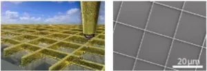
To address this dilemma, the ETH team has developed a technique to produce a transparent electrode based on the use of a 3D printing technology. The process creates a grid made of gold or silver ‘nanowalls’ on a glass surface.
The walls are very thin, with a width between 80 and 500 nanometers. These walls are perpendicular to the screen and two to four times taller than their width. As a result, the grid is highly conductive but virtually invisible to the eye. To put this accomplishment into context, the new electrodes have a higher conductivity and are more transparent than the ITO electrodes used in, for example, the current generation smartphone touchscreens.
Nanowalls are fabricated utilizing a form of 3D printing called electrohydrodynamic ink-jet printing. The process begins by suspending gold or silver nanoparticles in a solvent. Ultra-small droplets of this metallic “ink” are drawn out of a tiny glass capillary tube by an electric field. The drops that come out of the tube are about ten times smaller than the tube’s aperture. The drops hang on the tip of the tube. By carefully balancing the composition of the ink and the electric field, the researchers have been able to get an even smaller droplet to form at the base of the attached drop. It is these secondary droplets that are used to print the nanowalls.
The solvent evaporates quickly, allowing a three-dimensional structure to be built additively, droplet by droplet. The nature of this process makes it possible to vary the height of the nanowalls during their fabrication.
The researchers report achieving metal grid transparent electrodes optimized for low sheet resistances (8 ?/sq at a relative transmittance of 94%) as well as optimized for high transmittance (97% at a sheet resistance of 20 ?/sq). These parameters can be adjusted to meet the needs of a specific application.
Electrodes fabricated using this new process should be particularly suitable for product applications that require a large touchscreen. This is due to the high conductivity of the electrodes.
The researchers suggested that the so-called “nanodrip” process can be less expensive than current methods used to produce touchscreens based on ITO electrodes. The reason is that fabricating ITO electrodes requires expensive vapor deposition equipment and a clean room.
The next major challenge in nanodrip technology will be to develop means to scale up the print process to the extent that it can be implemented in a factory setting. To achieve this, the researchers are working with colleagues from ETH spin-off company Scrona (Zurich, Switzerland).
Readers that wish to learn more about nanodrip transparent conductor technology are referred to three articles on the subject that were recently published by the ETH team. There are available on-line. The first, second and third articles can be accessed with these links.
– Arthur Berman
ETH Zürich, Patrik Rohner, +41-44-632-2934, [email protected]