Yesterday, we looked at the way that Aledia is developing its Nanowire microLED technology. Today we look at the cost issues and practicalities.

The next list shows the many approaches that have been proposed for mass transport, but only the simple pick and place has been used commercially. There’s a nice diagram available online here on the Nature website.
- Elastomer stamping
- Electrostatic/electromagnetic transfer
- Laser-assisted transfer
- Fluidic self-assembly.
The following table shows the spec of the recently announced Jade Bird Display 0.3” 640 x 480. What these new displays indicate is that µLEDs can be designed to 1.7 µm. This table is used to determine the size and pitch of the pixels f and to calculate the area needed for a 4K and 8K resolution. Columns 1, 2, 3 are from Jade Bird, which use a 0.3” diagonal and has a 640×480 resolution. Column 4 shows the specs if the panel were full color. Columns 5 and 6 shows the number of pixels and area for 4K and 8K, respectively.
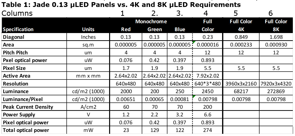 Click for higher resolution
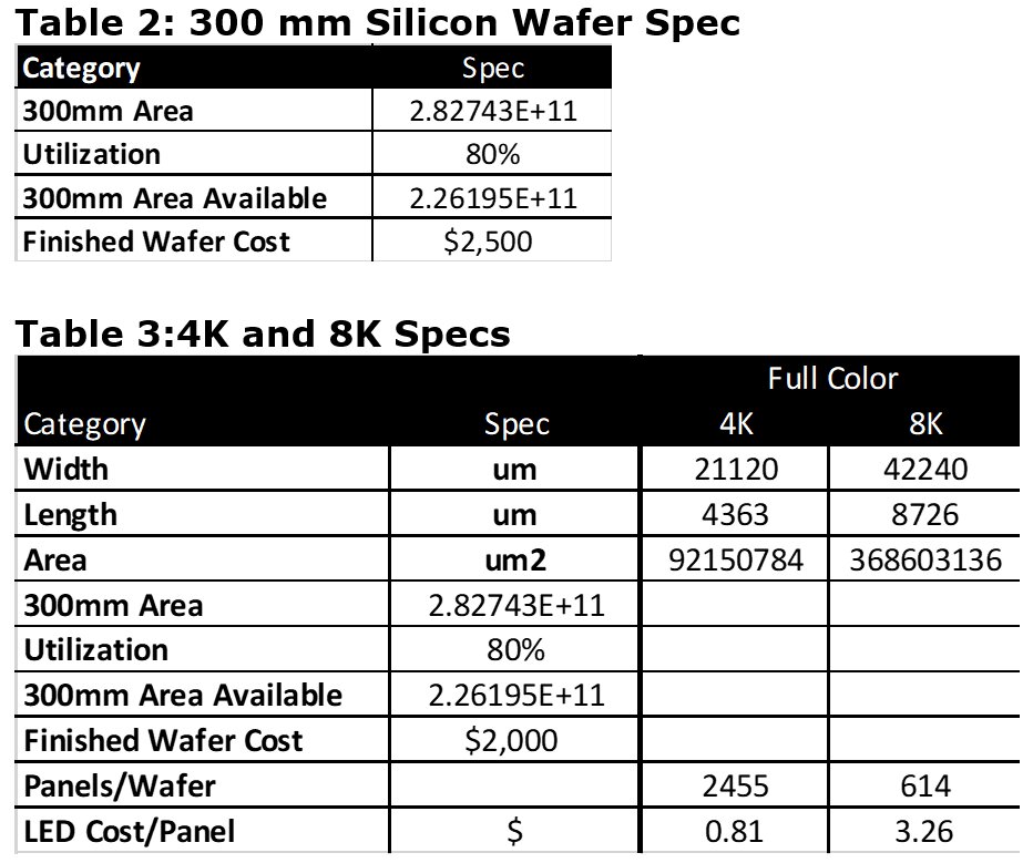
To determine the cost of the µLEDs, we use the area of the 4K and 8K µLEDs, divided into the 300mm available area and the multiple by the finished wafer cost, which results in $0.81 per 4K device and $3.26 for an 8K device.
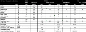
The next table shows the cost elements of a 65” 8K OLED TV panel as built in 2021. Costs are then projected thru 2025. In addition, the cost breakdowns for OLED IJP and QLED (LCD) TVs are shown. As we’ve seen, there are many solutions for transporting µLEDs between LED wafers and displays wafers, but there are no commercial high volume solutions today. Further Aledia will not disclose their technology, performance or costs. Because of this, we chose to calculate the capex available for the task. In the case of OLEDs its was $4.4b, for IJP, $3.1b and QLEDs, $2.2b. Clearly this level of capex is large enough to suggest the task is possible.
Table 4: 65” OLED and LCD Panel Costs. Click for higher resolution
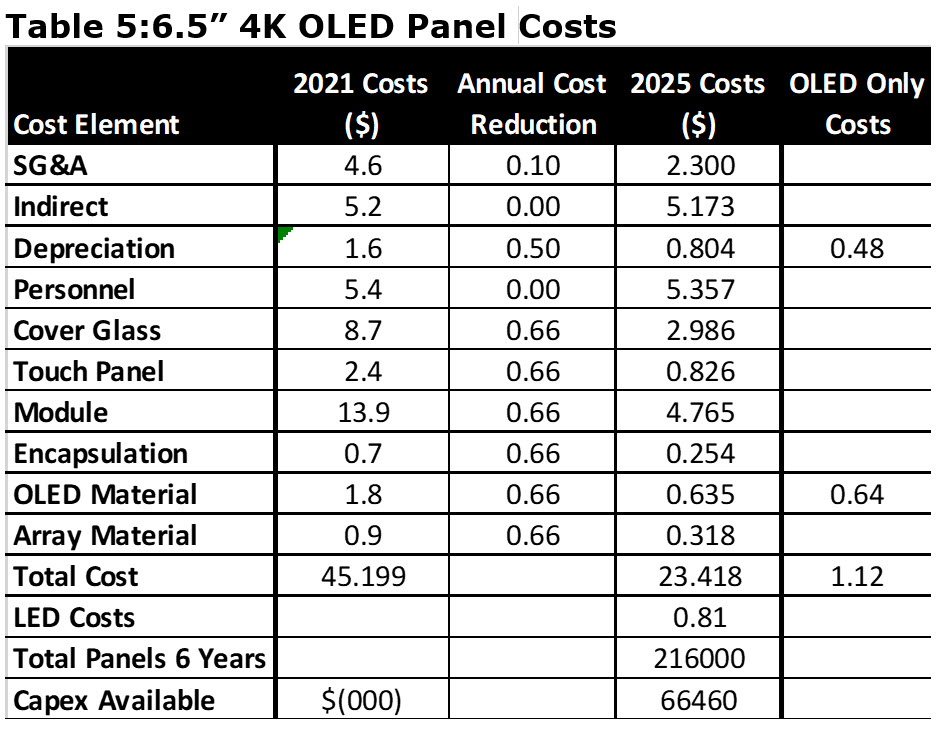
For OLED-based smartphones, the results are quite different. The µLEDs are close to the OLED costs such that there is only $66m in capex available for transport, making it unlikely that a cost effect solution will be developed.
 Source: OLED-A
Aledia’s solution should be competitive with both OLED and QLED TVs, which could be a 50m panel market in 2025. However, microdisplays can also be made using blue µLEDs and a color converter. Using a color filter, the efficiency would drop by 2/3rds, such that the spec’d 68m cd/m² would drop to ~32m cd/m² and at least 1 extra µLED per pixel would be required for redundancy, increasing the cost by ~$1,00 for 8K. Since the luminance requirements for TVs in 2025 are likely to be 2000 cd/m² with peak levels at 10,000 cd/m² for 1 mm² areas to support HDR, it would be well within the capability of blue µLEDs w/color filter, such that any feasible transport system would apply.
In the TV application µLED’s high luminance and longer lifetime are saleable differentiators against OLEDs. The higher wall efficiency is also, but unless the government makes it an issue, it’s not relevant. As to color, OLEDs have always been able to meet whatever spec is relevant. µLED’s faster response time is unlikely to make a difference for TV watching but could influence gamers.
The Risk to Capital
Aledia’s investors are being asked for risk capital to provide a solution that may not be the typical order of magnitude improvement over what already exists. Investors may also double or triple their investment or get diluted to get to mass production. Moreover, by 2025, the industry will be six years into what is likely to be a 9-year life cycle for 8K (similar to HD and 4K) and another 4X increase in resolution could substantially reduce the cost benefits of µLEDs over OLEDs.
On the positive side, Aledia’s approach would make a big difference in the power consumption of micro displays for AR, where high luminance > 50K cd/m
Aledia’s investors are being asked for risk capital to provide a solution that may not be the typical order of magnitude improvement over what already exists. Investors may also double or triple their investment or get diluted to get to mass production. Moreover, by 2025, the industry will be 6 years into what is likely to be a 9-year life cycle for 8K (similar to HD and 4K) and another 4X increase in resolution could substantially reduce the cost benefits of µLEDs over OLEDs.
On the positive side, Aledia’s approach would make a big difference in the power consumption of micro displays for AR, where high luminance > 50K cd/m² and power consumption of less than10 mw would be highly desirable. But the market is immature and Anania doesn’t believe it could justify the required investment. A more compelling approach would be to build the NW on a silicon substrate that already contains the TFTs and capacitors to drive the NW LEDs. Then the transport system could transport the pixels and, TFTs and capacitors in unison, eliminating the active matrix capex. (BY)
Barry Young is the CEO of the OLED Association