I’m going to start today’s Display Daily, but getting out, up-front, that I am no expert in optics. However, the topic has been getting more and more interesting recently and because of the critical aspects of optics to AR & VR, I have been keeping more of an eye open for developments.

Some six years ago, a proper expert on optics, Karl Guttag, wrote a Display Daily article that was entitled “VR and AR Head Mounted Displays – Sorry, but there is no Santa Claus“. He highlighted the challenges that were not directly related to the device itself and a number of those were about optics. I have also said many times over recent years that “There’s no Moore’s Law for optics”. In fact, I remember talking to an optical engineer at a Projection Summit some years ago that highlighted that environmental issues, including the issues from the use of lead in glass, were actually making some problems harder to solve.
However, at the recent DSCC AR/VR Conference (which is still available online), Applied Materials said that they see optical nanostructured waveguides as a strategic technology. The firm is a leading supplier of equipment for semiconductor and display manufacturing, so when it says something like this, it’s worth having a look at what is happening. Now, Moore’s Law and the consequent massive cost savings and improvement performance depends on squeezing more and more transistors into the same space. That doesn’t work in optics (or FPDs, generally, although cramming pixels closer together using microdisplays can mean a smaller etendue angle to help couple the light into optical systems. Check this DD My Etendue Story from several years ago for more on this topic).
Although optics hasn’t, up to now, depended on this kind of technology, being mostly about polished and coated surfaces and materials, the kind of manufacturing used in semiconductor manufacture are now being applied to improve optics. Our oldest article on this kind of ‘metamaterial’ goes back to one by the much missed Matt Brennesholtz in 2014. (TTop LED and Laser Technologies for Displays from 2014). Metasurfaces are optical surfaces that incorporate nano-structures that can manipulate light (New Technologies for 3D and More).
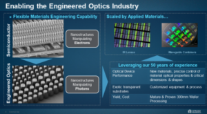
At the DSCC event, Robert Visser of Applied Materials, and a distinguished display scientist (and a recipient of an SID Fellows Award in 2021), pointed out that semiconductors involve nanostructures that manipulate electrons, while the new metamaterials mean creating nanostructures to manipulate photons.
One of the key advantages of this kind of optical structure is that you can develop flatter optics and that’s a real advantage for AR and VR. At the DSCC event, Visser’s colleague, Ludovic Godet presented on how the firm is using the nanoscale structure creation techniques from semiconductors to develop and improve the waveguides that are used in AR applications to transfer light from the display device to the eye. A waveguide in front of the eye has to be a flat optic, however it works, but there are other applications that can really benefit from thin and flat optics, where they were bulky before.
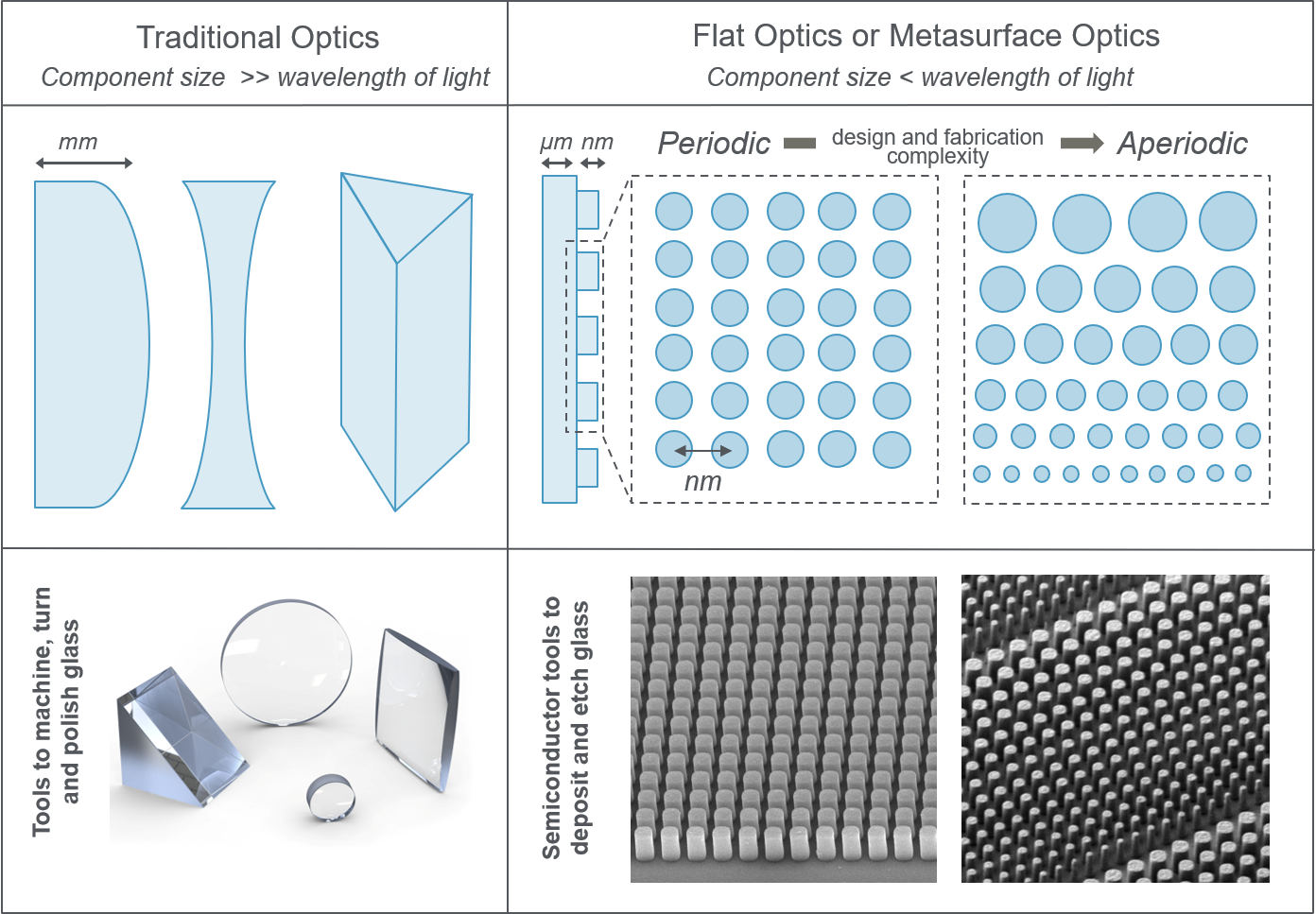 Image: Applied Materials Blog
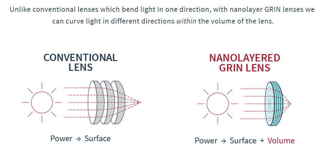
In recent months, I have, in trawling the web for our What Bob Saw subscribers, I have found a number of other new developments from groups that are looking to radically change optics. For example, in October, I reported on new technology from Peak Nanosystems of Ohio which has just got funding to further develop its ‘GRIN’ (GRadient INdex) technology, which uses nanolayers of polymers applied to lenses to change the refractive index of the lens at different points on its surface. The company says that its technology could make binoculars 10 times thinner and 80% lighter than traditional glass lenses.
Back in the summer, we reported on several developments in making thin optics. A group from Ottowa in Canada published an article in Nature describing what it calls a ‘spaceplate’, made using metasurfaces and metalenses.
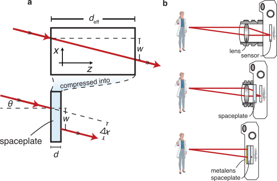 Operating principle of a spaceplate. a, A spaceplate can compress a propagation length of deff into a thickness d. For example, a beam incident on the spaceplateat angle ? will emerge at that same angle and be transversely translated by length w (resulting in a lateral beam shift ?x), just as it would for deff of free space. b, Adding a spaceplate to an imaging system such as a standard camera (top) will shorten the camera (center). An ultrathin monolithic imaging system can be formed by integrating a metalens and a spaceplate directly on a sensor (bottom). Credit: Orad Reshef and Jeff Lundeen u Ottawa / Nature Communications.
Around the same time, microdisplay maker, Kopin, said that it has developed an all plastic ‘pancake’ lens that uses aspherical lenses and special plastic materials that have almost no birefringence in a folded optics configuration. (Kopin Corporation Announces All-Plastic Pancake® Optics with Excellent Performance)
Just a week before that, we reported that a group from Cornell’s School of Applied and Engineering Physics and Samsung’s SAIT have made a new metalens that can be focused using voltage instead of mechanically moving its components. That’s intriguing, although the current R&D project only works on a single wavelength of red light at the moment. You can find a paper detailing the research in the American Chemical Society’s journal Nano Letters.
So while it still seems to be true that “there’s no Moore’s Law for optics”, it may be more accurate to now say that “optics can really benefit from the technology developed to support Moore’s Law”. (BR)