Over the years, I have heard many talks about different methods of depositing RGB OLED materials. The lack of a good and shared method for patterning the RGB OLED materials on large substrates has been one of the key barriers to wider OLED TV development.

On the face of it, you might have thought that putting the RGB dots onto a glass substrate should be relatively simple, but it has not proved that way.
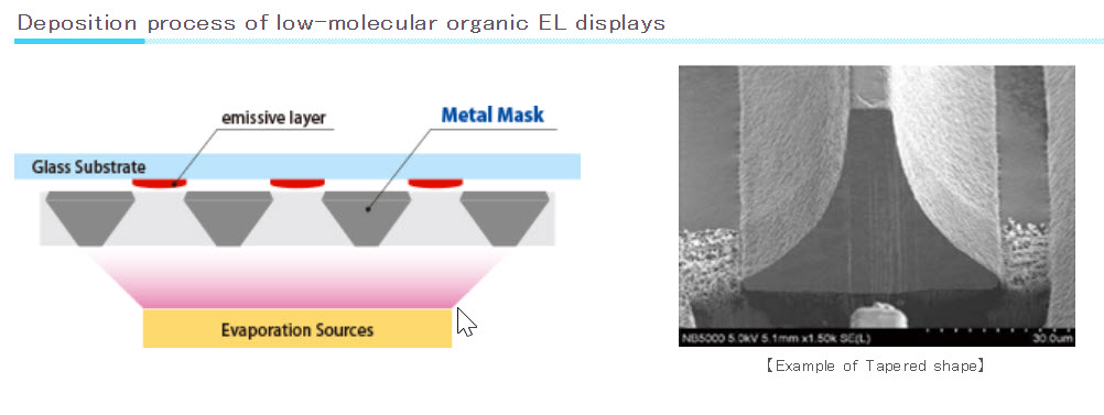
Many years ago, Kodak and Sanyo Kodak, were trying to develop larger OLEDs. I had heard a rumour that Kodak had hit a road-block in its chosen method of putting the materials onto the glass. Kodak was using vapour deposition with a shadow mask. The materials were put into a vapour in a chamber and a shadow mask (a metal stencil also known as a ‘fine metal mask’ or FMM) was put on the glass and where the vapour went through the glass, it deposited the OLED emitter. This had to be done three times, with slight offsets to pattern the materials for red, green and blue.
 Fine metal masks – Image:Toppan printing
I had heard that Kodak was struggling to do this above about 15″ or so diagonal because of the mask sagging and other challenges and by chance I was due to meet the firm at a trade show. “So”, I said, “I hear that you are having trouble making OLEDs above 15 inch. Is that true?”. To my complete surprise, as no US public company had ever admitted a negative point to me with a clear simple statement, “Yes”, they said.
The key reason for this was the difficulty of getting the three RGB elements accurately aligned. For small high resolution displays for headset , the accuracy might need to be 2um, although bigger and lower resolution, there is a bigger tolerance. However, the invar metal masks typically are thicker than the ideal and cannot be accurate enough. If the pixels are not accurate enough and spread out, the different colours can mix, degrading the image quality. (That’s a very short description of a process that has had a lot of study!)
As far as I know, FMM is the process for all the OLEDs used in smartphones and is certainly used by Samsung. However, Samsung has also struggled to get FMM to the kinds of sizes that would be needed for TV applications.
Waste is Also an Issue
One of the key disadvantages of this method of depositing the materials is that almost of the material is wasted as it doesn’t land through the holes, so companies have also worked on other ways of putting the OLEDs on the substrate. A factor in this is that the materials themselves are very, very expensive, so it’s a shame to throw them away! As long ago as 2012, Ross Young, then of DisplaySearch, but now with DSCC, reported at SID that 97% of the OLED emitter material and 75% of other materials were wasted in vapour deposition.
Ink jet printing was seen as a key way of doing it, but the accuracy is tricky and it’s really hard to get the shape of the pixels exactly right. Kateeva of the US has said it can do it for TVs and Semes in Korea (related to Samsung) also has equipment available, but nobody yet has inkjet printing of OLEDs in mass production, although pilot lines exist. I would be careful about betting that it will be in mass production soon. I reported that CDT had teamed up with Litrex in 2001 to develop the technology and a few years later we reported that CDT was ‘close to a breakthrough’ with Epson.
A variation of this was nozzle printing, developed by Du Pont and DNP, but that didn’t happen. It could not make very small pixels, so was only for TVs, and probably would have struggled with 4K and 8K sets in the long term. UDC continues to promote a not dissimilar approach called Organic Vapour Jet Printing (OVJP).
A challenge of all of the Du Pont and IJP approaches has been that the OLED material needed to be soluble and put into an ink or other liquid. UDC says that its version doesn’t need this.
Other ideas included LITI (Laser induced thermal imaging) around 2004 and onward, which Samsung wanted to use. The OLED material was to be deposited on a film, then transferred to the display with a laser. At one point, it was reported that Samsung planned to use FMM for blue and LITI for red and green. However, it didn’t happen.
(LG solved the problem of patterning by not patterning! It uses multiple layers of unpatterned OLED materials to create the emitter and a colour filter to produce RGB, but this wastes most of the precious light. The approach was developed by SK Displays, in desperation, when it was unable to get yields of RGB OLEDs nearly 20 years ago. I have previously described this as inelegant, but have been called to task on that! SK did make some displays that way vs almost none using RGB and LG is unique in developing mass production large OLEDs that way so far, so perhaps I was a bit harsh!)
Now, Photolithography
Anyway, all of this brings me back to Imec. At IDW this week, the Belgian research institute, working with the National Cheng Kung University in Tainan, Taiwan and the Holst Institute in Eindhoven, the Netherlands, presented a paper on an approach using photolithography – the process used to make silicon chips and LCD, OLED and other active matrix displays. That’s not a new idea and has been used in OLED microdisplays – indeed, I reported on work on that topic by Imec and Fujifilm back in 2013 (and reported on work on this topic by Merck in my SID report in 2006!)
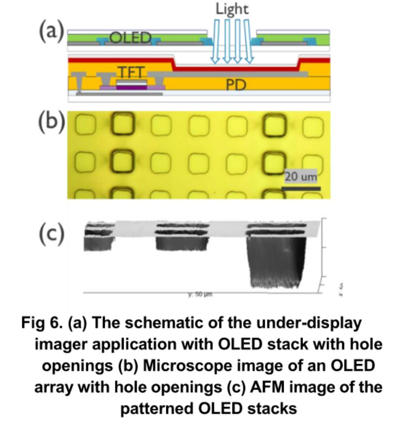
The work at Imec has partly been driven by the need to have space between the OLED pixels to allow the integration of sensors, such as fingerprint sensors, under the display.
Tung Huei Ke, R&D project leader for sensor technology, at imec, told Optics.org,
“Photolithographic patterning of OLED was extremely challenging because of the chemical incompatibility of the photolithography chemistry to the OLED materials. Also, the sensitivity of OLED materials to water and oxygen in a conventional photolithography environment was a major difficulty”.
The challenges are made more difficult because, for RGB, the process has to be performed three times. This is where the new paper shows something of a breakthrough, with “very low device lifetime degradation after the photolithography patterning process”. The paper highlighted that the OLED characteristics of once and twice patterned OLEDs were ‘quite similar. Both cases show a driving voltage of 6.6V and an efficiency of 86-87 cd/A’. The lifetime curves (T95 > 200 hours) of non-, once- and twice-patterned devices are basically the same.
The key factor in this development is that large area photolithography is a very well understood process for the display industry, so although you would need to have the right kind of production flow if you wanted to put the concept into mass production, you could exploit the knowledge of photolithography. (BR)
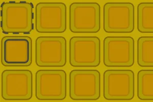
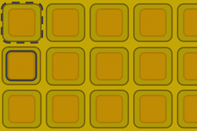 Microscope image of OLED ‘islands’.