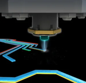
Researchers investigated the mechanism of subtractive contact patterning (SCP) and demonstrated its application in creating high-resolution organic light-emitting diodes (OLEDs). SCP is a method used to create patterns on thin films of organic semiconducting materials, which are essential components of OLEDs and other organic electronic devices. The research was done by a group out of the Department of Creative Convergence Engineering, Hanbat National University, South Korea, and published in the ACS Applied Electronic Materials journal.
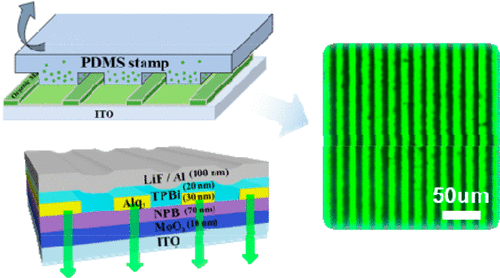
The researchers applied SCP to various types of organic semiconducting thin films, including crystalline thin films and amorphous small molecule thin films. They found that crystalline thin films generated patterns through a delamination mechanism, while amorphous small molecule thin films generated patterns via a diffusion mechanism. In the diffusion-based pattern generation, they observed that higher processing temperatures and longer processing times led to deeper pattern depths, with the patterning speed being proportional to the temperature in an exponential function.
The study showed that SCP could be applied to doped small molecule-based thin films and, to a limited extent, to polymer thin films. The researchers successfully fabricated high-resolution OLED patterns less than 10 μm wide using the SCP process without negatively affecting the device performance. They also demonstrated the application of SCP to flexible and curved thin films, indicating its potential use in roll-to-roll manufacturing processes.
This study adds to the existing body of research by providing a comprehensive analysis of the SCP process and demonstrating its effectiveness in creating high-resolution OLEDs. The insights gained from this research can help improve patterning techniques for organic electronic devices, enabling the development of more advanced, miniaturized, and cost-effective products in the future.
Patterning Techniques Scale as Needed, or Not
The additive and subtractive approaches to micro and nano scale manufacturing offer distinct advantages and limitations. Additive manufacturing, with its layer-by-layer deposition process, promises greater design flexibility, reduced material waste, and the potential for more environmentally friendly production methods. However, current additive techniques face challenges in achieving the high resolutions and broad material compatibility offered by well-established subtractive processes like photolithography. Conversely, subtractive manufacturing processes have achieved remarkable precision and material versatility through decades of development, enabling the production of complex micro and nano devices. Nevertheless, these processes often require substantial financial investment, energy-intensive infrastructure, and can generate significant amounts of waste. As additive manufacturing technologies continue to advance, a hybrid approach that combines the strengths of both additive and subtractive methods may emerge as the optimal solution for micro- and nanoscale device manufacturing, providing cost-effective, energy-efficient, and environmentally sustainable production processes.
Display manufacturers often develop strategies to overcome challenges or optimize processes to meet their production needs. The suitability of a patterning technique for large-scale manufacturing depends on various factors, including the specific requirements of the devices being produced, the cost, and the trade-offs between different techniques. Below is a summary of some common patterning techniques, their resolution ranges, advantages, and disadvantages.
| Technique | Resolution Range | Advantages | Disadvantages / Limitations |
|---|---|---|---|
| Photolithography | Varies, down to sub-micrometer | Widely used, precise patterning | Challenging for organic materials, chemical and thermal issues |
| Inkjet Printing | Tens to hundreds of micrometers | Cost-effective, large-area, flexible production | Not ideal for high-resolution, small pixel sizes |
| LITI (Laser-induced Thermal Imaging) | Down to a few micrometers | High-resolution patterning, suitable for OLED displays | May involve more complex equipment and setup |
| μCP (Microcontact Printing) | Varies, typically not the highest resolution | Low-cost, relatively simple method | Limited resolution compared to other techniques |
| Shadow Masking | Down to a few micrometers | Direct patterning, no need for photoresist | Challenging for large-scale manufacturing, mask durability and alignment issues |
In some cases, manufacturers may combine different patterning techniques in their production process to leverage the strengths of each method and overcome the limitations of others. For instance, photolithography can be used for creating fine patterns on the substrate, while inkjet printing can be employed for depositing large-area organic layers. Essentially, the race to volume manufacturing requires companies to be agnostic about processes, and focused on results, but there is always a Holy Grail, find the process that will take into the quantum realm so that capex investments and research methodologies can be fine tuned and more efficient.
Reference
Lee, S.-H., Park, H.-L., Lee, S.-H., Noh, E.-K., Hwa, S., Lee, J., Lee, J.-H., & Kim, M.-H. (2023). Systematic Investigation of Subtractive Contact Patterning for High-Resolution Organic Electronic Devices. ACS Applied Electronic Materials. https://doi.org/10.1021/acsaelm.3c00080