Six companies presented in this morning session. rpVisual’s James Fife gave an illuminating presentation on the mounting of LED video walls. He described all the ways such mounting projects can go wrong and many of the steps that are needed to properly design and install a mounting solution.
There is far more complexity to the job than we had imagined prior to this talk. A 22.6’ (6.86m) wide LED screen must be assembled with just 2mm of tolerance over this span, so you want to anchor to something that will not move more than this, for example. And, when mounting fine-pitch screens, the gap between cabinets must be maintained to 0.05 mm or else you will see dark lines. Fife also touched on heat management too as this must be considered in the mounting solution as well.
The clear take away – get a professional who has a lot of experience in mounting solutions.
ZhongShen Luo from Nanosys started out with a bit of history on quantum dot development, some of the pros and cons and comparisons with OLED and LED displays. MicroLEDs are being explored for AR/VR as well as direct view displays because of their small size, high efficiency and high brightness capabilities.
Creating an RGB microLED can be accomplished two ways. Once is to fabricate blue and green microLED in GaN and red LED in GaAs. The other approach is to fabricate a wafer of blue LEDs and add a color conversion layer for the red and green. Using quantum dots is one promising way to do the color conversion.
Microdisplays for AR/VR may be able to pattern the device at the desired pixel pitch in GaN, but other displays for direct view applications will need to change the pixel pitch via some mass transfer technology. He showed some data suggesting that doing a mass transfer with microLED with integrated color conversion would be a much higher yielding process than the discrete microLED mass transfer approach.
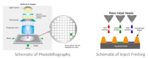
However, creating quantum dot materials that can stand the high flux loads and depositing them at the small pixel pitches needed for MicroLED are current challenges. For manufacturing, Luo sees two viable approaches: ink jet printing and photolithography – and Nanosys is working on both approaches. Inkjet is an additive process so is more material-friendly. Subpixels with a size of 180 x 580 microns is the current target with a red, green and clear pattern. For the photolithographic subtractive side, Nanosys and a partner have demonstrated line widths as small as 3 microns.
George Powch from VerLASE used his time to describe the RGB microLED solution they call Chromover. The Chromver technology is a separate patterned substrate that would be bonded to a blue LED wafer or a blue VCSEL array. Conversion of the blue light to red and green is done with separate quantum well sub-pixel structures. The acceptance angle of the ChromOver layer is fairly narrow, ±15º, so light outside of this angle is confined to the carrier substrate and waveguided to the edges.
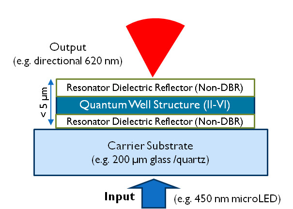
Powch said these structures, which are a form of optically pumped resonant cavity LED, are highly efficient, absorbing 98% of the blue light while simultaneously meeting output resonance conditions for the red or green. All other known resonant cavity LEDs are electrically pumped, but theirs is optically pumped. He said their structure leads to 5-10X the typical light output of a quantum well structure because of the resonator design.
Moreover, the output cone can be defined as well, so the light can be highly directional with low étendue, which will be important for any AR/VR application. Other color conversion schemes are omni-directional emitters.
So far, VerLASE has demonstrated green emission at 520nm with a blue pump at 450nm. Powch says the spectral line width is a design factor and can be very narrow – as small as 4 nm.
Powch says the technology can be made with two conventional processes: MBE and optical coatings, so is readily scalable.
Eric Virey from Yole provided their market assessment of the microLED market opportunity. He noted that there is considerable interest in the microLED maket with over 140 players on their list including majors like Apple, Foxconn, Sony, Samsung, LG BOE, Intel and more. Patent activity is increasing too.
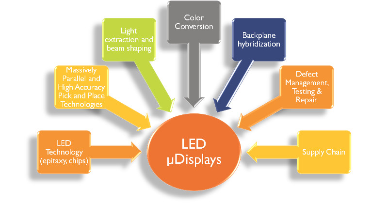
He talked about the clear benefit of microLEDs in direct-view and microdisplay-based applications and then turned to discuss some of the challenges. For direct view displays, using a traditional one-at-a-time pick and place technique would take about 41 days to create a 4K display. Obviously, this is not acceptable, so a mass transfer technique is needed. He pointed to an important milestone that has just been reached by PlayNitride: the ability to mass transfer 200K microLED die per second, thus exceeding what he thinks is a minimum rate needed for consumer devices of 30K device transfers per second.
There are currently about 6 different methods being explored for mass transfer. But that is just one of the key challenges to commercializing microLED displays, as shown in the graphic below.
Virey then turned his attention to some of the applications for microLED such as smartwatches, AR/MR headsets, HUDs or RPTVs, large displays for ProAV or Cinema applications. These are all in various stages of development with all facing challenges before they can come to market.
For TVs, Virey sees some interesting possibilities because the cost of a microLED TV scales with the number of pixels, not the area as it does with OLED and LCD TVs. As a result, a 55” TV could cost the same as a 110” TV. He also discussed a kind of hybrid TV solution where a conventional backplane is fabricated on later generation fabs with microLEDs placed on top as the frontplane layer.
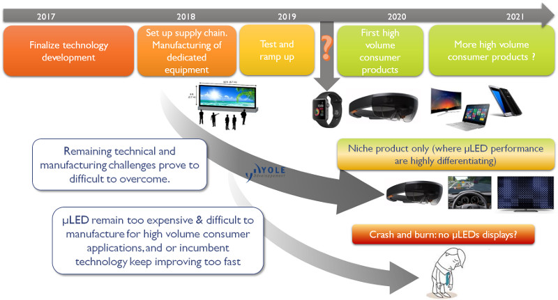
He concluded by noted that there are so many “moving parts” in the microLED market and so many challenges that it is hard to predict the future. Therefore, he hedged offering three scenarios as outlined in his graphic below.
Heng Liu from SiliconCore was next and talked about more conventional LEDs and applications. He said LEDs are driven with a pulse wave modulation (PWM) scheme and can respond to nano second scale pulses, which is needed to control very low light levels. However, not only is it difficult to generate ns pulses, but the parasitic capacitance in the PCB with an array of LEDs leads to a non-square pulse shape that will vary based upon the distance from the driver. That makes it very hard to control low level light with any uniformity. As a result, the common anode approach must use longer pulses – on the order of 500 ns to ensure uniformity, which means a sharp step from no light to the first light level. This may be acceptable for digital signage, but it not for cinemas and simulation applications.
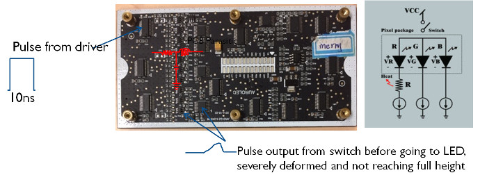
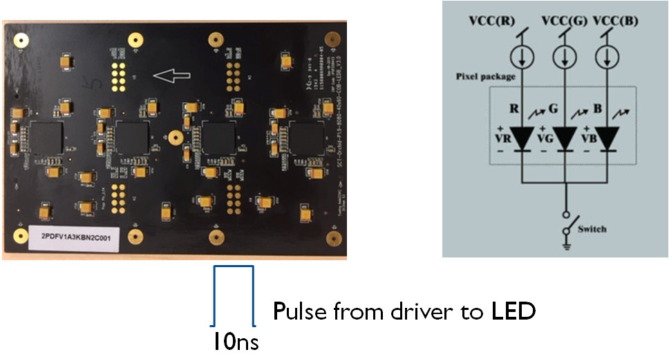
SiliconCore has a solution – their common cathode approach coupled with a new LED driver which has been optimized for control of very low light levels (SiliconCore Promotes Zach Driving). It is able to deliver clean 10 ns pulse over the full PCB with good uniformity. The trade-off is the need to have three separate power supplies.
LED modules can be constructed with Surface Mount Device (SMD) LEDs or Chip On Board (COB) mounting techniques. The company has demonstrated this capability with a 1.9 mm prototype using COB technology. (although I have heard that this is taking longer to roll out in production than hoped – Man. Ed.)
Finally, Gary Feather from Nanolumens focused on using LEDs in the cinema market. He started by noting that the cost of an RGB laser projection system with 4K resolution is in the $200K to $350K range which means a cost per pixel of around $0.03 cents – which should be the LED target as well. This is within reach and he thinks and that by 2019, LED cinema screens could reach 20% market share of new sales (by revenue).
While LEDs for use in cinema have many potential advantages, including a real HDR capability, there are many unanswered questions that need to be addressed to move the market forward (pixel pitch, fill factor, fixed pattern noise, operation at low luminance, color and gray scale uniformity, color volume, elimination of visible seams, EOTF, cooling, test and repair and 3D). But there were even more items on his list of things to address before LED cinema screen can go mainstream.
In the panel session, moderator Chris Chinnock asked the speakers about the use of LEDs and microLEDs in 2020. Several think that they will be in home-based products by 2020; Powch thinks they will be in early AR headsets; Feather sees a price drop of 20X coming, while Liu thinks microLEDs will be in wearables by then. These are quite optimistic forecasts by these experts. – CC