EV Group (EVG) of St. Florian, Austria and a supplier of wafer bonding and lithography equipment, together with the Korea National NanoFab Center (President Jae Young Lee, NNFC), a nano-technology R&D infrastructure for academia, research institutes and the industry, has developed improved transparent nanostructured anti-reflective coatings for next-generation displays. The ongoing work has been carried out within a joint-development program (JDP) established between the two partners in November 2015. This collaborative research has been partly funded by the Nano-Open-Innovation-Lab Project of the NNFC.
VG and the NNFC say that they have successfully demonstrated an anti-reflective coating with excellent structure replication that provides over 97% transmittance and a surface hardness of 3H, which is superior to most other polymeric coatings, according to the companies. By contrast, current commercial thin-film coatings only provide up to 92% transmittance, they added. The JDP partners achieved these results by applying EVG’s SmartNIL technology on 200-mm round substrates using a polymer material developed by the NNFC. This material was developed for performing a reversible nano molding process at the NNFC, and is compliant with commercial standards for display coating.
EVG and the NNFC plan to promote these results to start partnerships with end-users that are interested in joining the JDP to help commercialize the new AR coating by qualif the technology for industrial use through the NNFC. The next phase is implementation of the process by EVG to high-volume panel manufacturing on large screen sizes, such as Gen 2 (370 mm x 470 mm) panels and beyond. EVG will supply equipment.
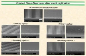
Details of the poster presented about the technology is available for download. However, the basic concept is that semiconductor techniques are used to create a nano-patterned mould that is used then to create a metal (or other material) working mould, which is in turn used to pattern the final mould.
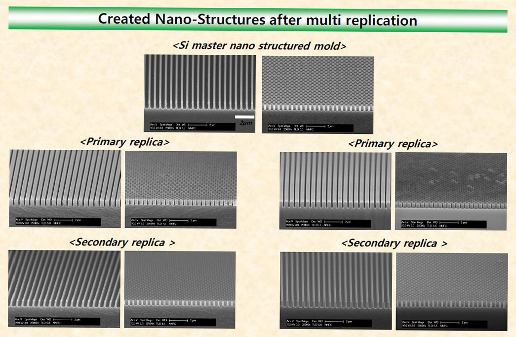 Semiconductor techniques are used to create an original pattern which is then used to create a secondary mould
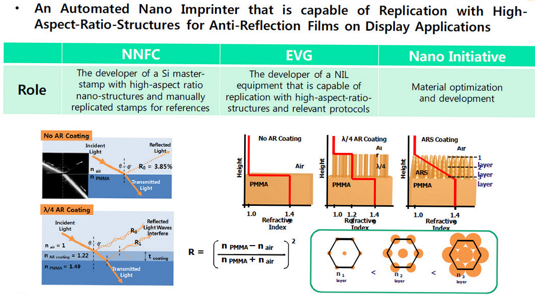
There are a number of applications for the concept, but one of the primary target markets is displaymakers as the companies have developed a pattern that can make a λ/4 coating that has a more complex structure than a traditional A/R coating. The structure means that there are, effectively, multiple different patterns according to the depth that is considered. At the top of the pattern, the points are relatively widely spaced, but much closer together close to the glass surface. (see diagram below)
In addition to this specific project, EVG and the NNFC plan to investigate other application areas leveraging nanostructures and NIL technology.
Analyst Comment
A/R coatings have been attractive in the way that they improve performance for more than 30 years. They are not new, but have invariably been too expensive. A printed process might well bring the cost down to be accepable for more widespread use. (BR)