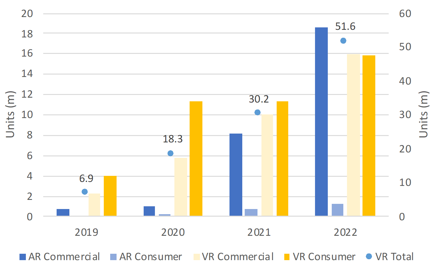
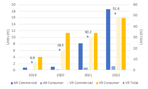
The VR/AR revolution has not materialized as expected by the illustrious leaders of Facebook, Apple, Google and just about all market researchers have had to drop their forecasts year after year. In 2019, 6.9m headsets were shipped, down 9.2% from IDC’s most recent forecast and down more than 50% from previous more optimistic forecasts. But the optimism remains as the major companies and an array of start-ups cumulatively invest billions in the technology.

Even with the misses, IDC now forecasts 52m headset by 2022, a 3-year CAGR of 96%. What’s at stake is a new paradigm in consumer and commercial computing. If we are to believe the Cook’s, Zuckerbergs and Pichais, the smartphone and the TV will be replaced by an ergonomic pair of glasses that deliver the digital and analog world simultaneously in harmony.
Forecast of AR/VR Headsets by Consumer and Commercial Use
 Source: IDC
Of course, the technology is not ready. Small standard high pixel density OLEDs have enabled VR but their ppi and luminance limits are insufficient for AR, which must operate in high ambient daylight. OLED microdisplays have been tried as they overcome the ppi limitation but the use of white emission with a color filter limits the brightness. MicroLED micro displays have been hyped as future solutions, but the costs and technical issues have delayed any product introductions.
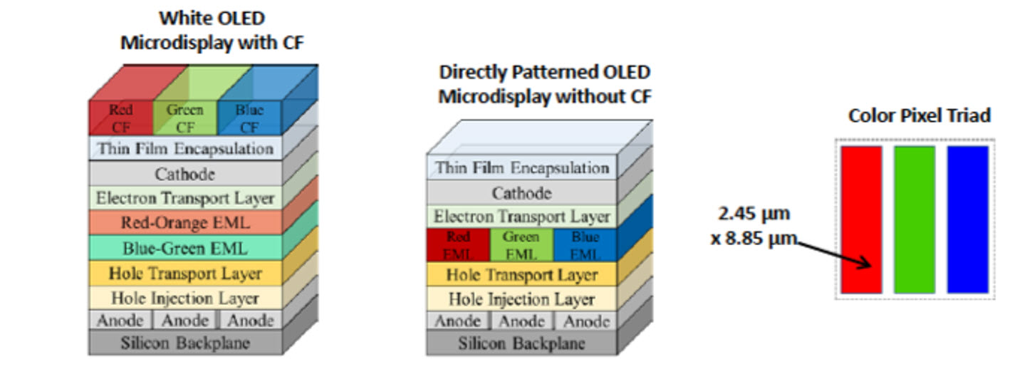
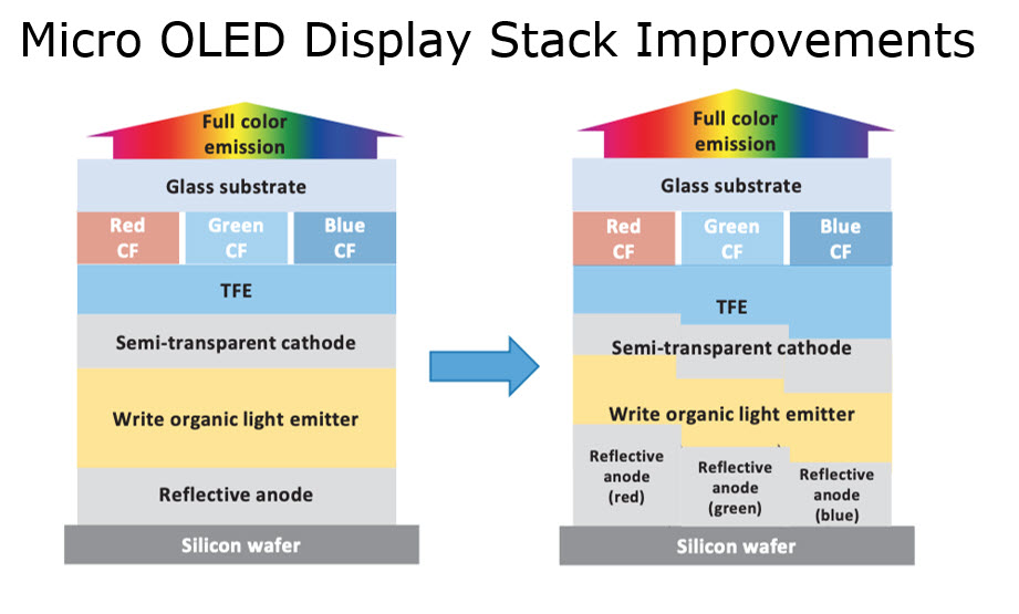
eMagin, a small OLED microdisplay manufacturer may preempt the over hyped microLED by solving the luminance and pixel density issue. They recently announced an OLED micro display with RGB stripe pixel layouts that used no color filters and produced ~7,500 cd/m2, the starting point for A/R devices The 0.9” display has a resolution of 1920 x 1200 and a ppi of greater than 2600 .eMagin uses direct patterning of the OLED emitter layers as opposed to previous designs, which used white (R,G,B) with a color filter. Kopin recently announced a high brightness OLED microdisplay but they used a duo structure, or two layers of each red, green and blue emitter to plus a color filter to achieve 1,000 nits.
Forecast of AR/VR Headsets by Consumer and Commercial Use
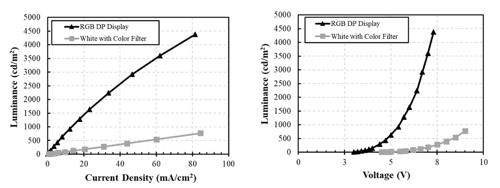
eMagin used a phosphorescent green and red and fluorescent blue materials. They were able to produce 1920 x 1200 devices on an 8” wafer with a 9.6µm as well as 9.3µm color pixel pitch. The devices achieve 6X more luminance at comparable current density and 20X more luminance at comparable voltage. Andrew Sculley, eMagin CEO indicated that their next goal was >10,000 cd/m2 in full color and could go to higher than 25,000 cd/m2, eventually. Andrew reported that 2 large well known OEMs had already contracted with eMagin to develop prototype VR devices. In a presentation at the 2018 OLED summit, Andrew compared the 2 device structures.
eMagin’s OLED Device Structures
More importantly, the current density and voltage vs. luminance shows 5 to 10 fold improvement using the direct patterned approach.
Direct RGB Patterning vs., WOLED Brightness Performance
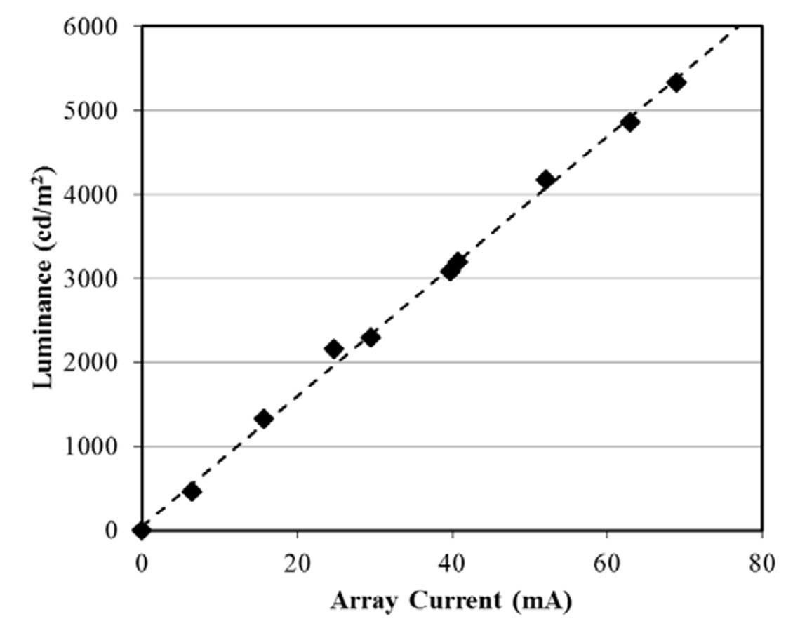
In Andrew’s 2018 presentation, he also included the linear relationship between luminance and the current passing through the array.
2K x 2K Direct Patterned RGB OLED Luminance vs. Array Current
 Source: USPTO
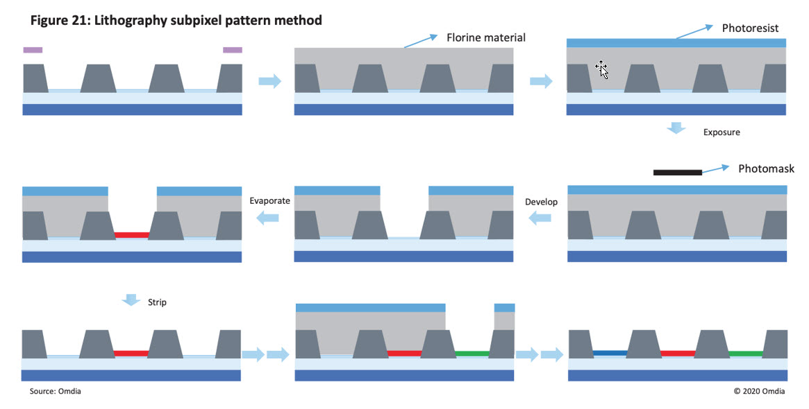
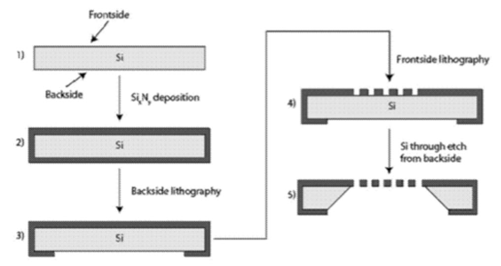
eMagin’s patent shows that they are using stencil lithography, where a high resolution SiNx mask is placed over the substrate and then the OLED materials are vacuum deposited through this mask. The shadow mask has nanometer scale features and the precision and accuracy to match the underlying transistor of the microdisplay. According to the patent, SiNx is deposited on both sides of a silicon wafer using CVD equipment.
The SiNx layer may function as an etch barrier on one side and a free-standing membrane on the other side. One side of the thin film is patterned and etched to expose the substrate for a subsequent through etch process. The other side of the film is patterned and etched to create the desired shadow mask pattern. The through substrate etch on the back side suspends the film, so it can be used as a shadow mask. In the patent application, they commented that they were able to do a near 1:1 transfer onto the underlying substrate, with the shadow mask pattern at 6µm and the width of the transferred pattern at 5.9µm.
eMagin’s OLED Direct Patterning Process
 Source: eMagin Patent Application 2015/0041793 A1
The shadow mask ranges from 50Å to 2µm with the aspect ratio between the film thickness and aperture geometry a consideration as deposition material will build up on the sidewalls of the shadow mask and cause distortion in aperture size, which can be altered as the ratio between film thickness and aperture opening increases. Other considerations include the anisotropic etch of the silicon substrate where the sloped sidewalls need to be taken into consideration for accurate membrane geometries. eMagin used a through wafer etch of a 315µm thick wafer and an additional 446µm needed to be added to the mask design to form the targeted membrane geometry.
The new process was given the name dPd to distinguish it from the color filter approach. At eMagin’s, Q120 earnings call they said, “Direct Patterning equipment has been upgraded and installation is complete. We are in the process of qualifying the equipment and validating the process. Progress has been very good, despite vendor delays due to the corona virus. We are expecting to fabricate full color displays in the second quarter.” With the announcement of the 0.9” micro display, they will have met their commitment.
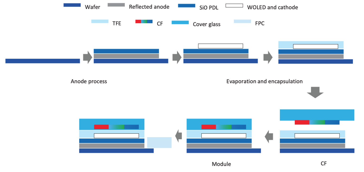
OLED Micro OLED Fabrication Process
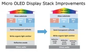
Micro OLED Display Stack Improvements
 Source: Omdia
Many thanks to Ross Young, founder and CEO of DSCC, who wrote about Andrew Sculley’s presentation at the OLED Summit and researched the patents enabling the direct patterning technique (BY)
Barry Young is the CEO of the OLED Association
Editor’s Comment
After publication, it came to our attention that a significant part of this article, including five of the figures, had been previously published in the DSCC Weekly Review. We apologise that this was not acknowledged and are grateful to Ross Young of DSCC for permission to continue to include this content. (BR)

