Researchers at the University of Sheffield have developed a new approach for fabricating MicroLEDs (μLEDs), microscopic LEDs with dimensions under 5 μm. The confined selective epitaxy (CSE) technique allows μLEDs to be formed directly during epitaxial growth instead of using conventional etching processes. Avoiding plasma damage provides substantial improvements to μLED performance and capabilities. It could be that CSE effectively addresses several challenges facing μLEDd, paving the way for efficient, customizable, and integrated μLEDs suited for next-generation displays.
Demand for MicroLED Displays
There is increasing interest in developing displays composed of arrays of microscopic μLED pixels for applications including augmented reality (AR), virtual reality (VR), smartphones, smartwatches, and televisions. With dimensions less than 100 μm, μLED displays can offer higher resolution, efficiency, and contrast compared to existing organic LED (OLED) and liquid crystal display (LCD) technologies. The global market for μLED displays is forecasted to reach $4.2 billion by 2025, with adoption in wearables, near-eye displays, and large format displays.
However, fabricating efficient and reliable μLEDs presents challenges. Conventional LED manufacturing uses photolithography and dry etching to form microscopic mesa structures. While suitable for larger LEDs, when applied to μLEDs under 10 μm, these etching processes damage the devices, reducing efficiency and yield. Additional sidewall passivation only marginally mitigates the damage. As a result, external quantum efficiency (EQE) of 5 μm μLEDs remains at just 1-5%, too low for practical use.
Beyond efficiency, etching also restricts certain μLED capabilities. Their broad spectral linewidth is ill-suited for high-resolution displays. Longer wavelength μLEDs like red are difficult to achieve since high indium content InGaN is hard to grow reliably. High leakage currents affect most devices. And integrating driver electronics requires complex transfer techniques incompatible with mass production. Overcoming these limitations is important for realizing μLED displays.
Confined Selective Epitaxy Technique
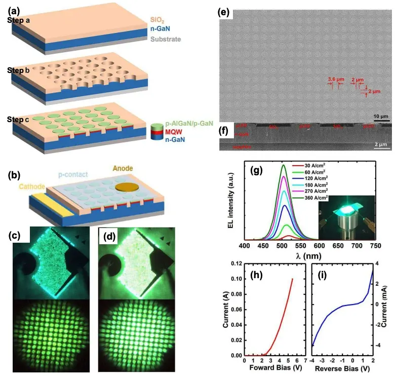
To address these challenges, the researchers developed confined selective epitaxy. Their technique uses metal-organic chemical vapor deposition (MOCVD) to directly grow μLED structures within oxide masks. This confined growth forms LED mesa structures during epitaxy without etching. The mask dimensions define the μLED size and spacing.
This process differs from regular selective epitaxy where films grow laterally over masks. Here, growth remains confined within the mask openings. The non-uniform deposition demands careful optimization of growth parameters. But confinement prevents plasma damage while allowing integration of μLEDs and electronics.
Advancements in μLED Performance
By avoiding plasma damage, CSE provides measurable improvements across key areas:
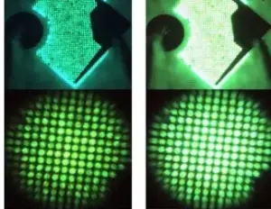
- Efficiency: CSE enabled 3.6 μm green μLEDs with a record peak external quantum efficiency of 9%, significantly higher than the 1-5% of etched μLEDs. Such improved efficiency makes μLED displays more viable.
- Wavelength Stability: CSE μLEDs integrated with a micro-cavity showed emission wavelengths stable over injected current. Confinement within the micro-cavity prevents shifts from quantum confinement Stark effects. This stabilization is important for high-resolution displays.
- Long Wavelengths: CSE promotes lateral strain relaxation within InGaN quantum wells, increasing indium incorporation. This allowed direct growth of red 642 nm μLEDs with 1.75% EQE, overcoming issues with conventional approaches.
- Leakage: Without etching damage, CSE μLEDs exhibited reduced sidewall leakage current densities down to 3×10⁻⁶ A/cm2. Lower leakage prevents unintentional pixel activation in dense displays.
- Integration: CSE enabled straightforward integration of μLEDs alongside HEMT driver electronics, avoiding complex assembly steps. An integrated HEMT-μLED reached speeds up to 1.2 GHz, demonstrating feasibility of self-contained display modules.
By jointly improving efficiency, speed, wavelength range, and integration, CSE represents a significant advance for μLEDs.
Enabling High-Resolution MicroLED Displays
The CSE technique provides a means to manufacture customized, efficient μLEDs for advanced displays. Adjusting the mask dimensions allows tuning of the emission color and pixel density. Dense arrays of efficient green, blue, and red integrated μLEDs with stabilized emissions appear feasible.
The team already showed μLEDs as small as 3 μm across. Initial tests suggest CSE remains effective down to sub-micron scales. Such small pixels could enable ultra-high resolution displays with over 1 million pixels per inch. CSE is straightforward and uses standard commercial epitaxy tools, facilitating eventual large-scale manufacturing. Combined with monolithic integration, CSE offers a path toward self-contained, scalable μLED display modules.
The CSE advance provides expanded capabilities as higher pixel densities and faster refresh rates are demanded. The team is also exploring integrating photonic components like waveguides alongside the μLEDs for advanced photonic circuits.
Reference
Cai, Y., Bai, J., & Wang, T. (2023). Review of a direct epitaxial approach to achieving micro–LEDs. Chinese Physics B, 32(1), 018508. https://doi.org/10.1088/1674-1056/ac90b5