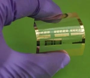
A team at the University of Wisconsin-Madison have developed a way to develop high-performance wireless transistors on rolls of plastic. These devices are able to operate at 38GHz, although 110GHz is feasible. Both power and data can be transferred wirelessly.
Circuitry was patterned onto the flexible transistor using a low temperature process. Single-crystalline silicon was placed on a PET (polyethylene terephthalate) substrate, using nanoimprint lithography.
Rather than using selective doping (introducing impurities in precise locations to enhance materials’ properties, such as conductivity), the researchers blanketed the crystalline silicon with a dopant. They then added a photoresist layer and used electron-beam lithography on the photoresist to create a reusable mould of the nanoscale patterns that they needed. This mould was applied to an ultrathin silicon membrane to create a photoresist pattern. The work was finished with a dry-etching processing, cutting nanometer-scale trenches in the silicon, following the pattern of the mould. Wide gates (functioning as switches) were added above the trenches.
It is said that this transistor consumes less energy than a conventional one. The production technique could enable a greater number of transistors to be applied to an electronic device, due to the extreme thinness of the trenches. The mould can also be reused, enabling scalability in roll-to-roll processing.

