The materials used in OLED devices can be very sensitive to oxygen and moisture. As a result, such devices needs to be isolated from the atmosphere. The means typically used to provide a protective barrier is an encapsulant.
When OLED devices first became available, the encapsulation material was commonly a glass or metal foil. These materials are, however, not suitable for the growing range of applications in which the device has a physically large area or that is flexible or transparent.
At this time, flexible OLEDs are encapsulated with a thin film based on combinations of metal oxides or nitrides in conjunction with polymer intermediates. The overall thickness of the thin films in such encapsulates range from a few hundred to a few thousand nanometers.
In the search for even better encapsulates, attention has included the study of graphene. The graphene related work reported in this article began in 2015. It is a collaborative project called Gravia that was undertaken in the UK. The team of researchers working on the Gravia project is headed by Abhay A. Sagade formerly in the Electrical Engineering Division, Department of Engineering, University of Cambridge (Cambridge, UK).
Recent results reported by the team can be found in an article entitled “Graphene-based nanolaminates as ultra-high permeation barriers.” It was published on October 23rd in the Nature Research Journal, 2D Materials and Applications 1, Article number: 35 (2017). A copy of the article is available online and can be found here.
This article contains a great deal of detailed technical information on the materials and process used to form the barrier film. The article also includes information on the techniques used to measure the properties of OLEDs that include the new barrier as well as the electro-optical and environmental properties of the resulting device. Here is a brief summary of the team’s most recent results.
In pure form, graphene is highly impermeable to gas. The trouble is that real materials are never entirely pure. In addition, while large area mono and few-layer graphene films can now be fabricated by Chemical Vapor Deposition (CVD), in practice, such atomic films are practically prone to defects along grain boundaries when produced in high volume. Attempts to “seal” these defects with the addition of a layer of polymer overcoat have not been completely successful.
The team’s latest research used Atomic Layer Deposition (ALD) and CVD to create scalable, large area, high quality, few-layer graphene/aluminum oxide-based nanolaminates.
In their article, the researchers report that the new means of “forming a nanolaminate structure by carrying out another graphene CVD run onto an AlO x /G/Cu structure effectively leads to further graphene layer growth fed by precursor permeation through the existing film.”
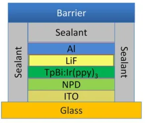
The configuration of the stack is illustrated in the figure below.
Schematic of stacks of layers in the new OLED configuration.
The researchers report that a “~10 nm barrier layer (about 30 graphene layers) is an effective encapsulation for OLED displays. The 10nm layer maintains a high optical transparency (>90 %) and high flexibility and show water vapor transmission rates below 7 × 10⁻³ g/m2/day measured over areas of 5 × 5 cm2.” The films were demonstrated to produce OLEDs that had a measured half-life time of 880 hours in ambient conditions.
A video illustrating the flexibility of an OLED device that includes the new barrier can be found at the end of this article.
The researchers state that their new approach is “comparable to existing commercial OLED encapsulation technologies.” They go on the comment that “While this proves the potential effectiveness of a graphene-based encapsulation for OLEDs, it is not clear whether this could be performed commercially at a low enough cost and at industrial scales.” –Arthur Berman
University of Cambridge, Abhay A. Sagade, [email protected]
ence